A reader left a comment under the article “Mitsubishi: High-Speed EML from High-Mesa Structure to Hybrid Glass Substrate with FC+WB”: “FC+WB — is that wire-bond-free?”
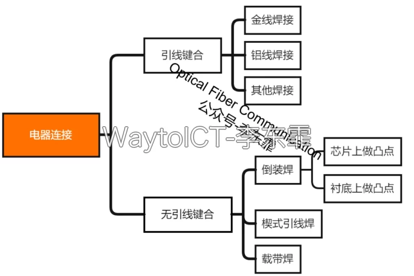
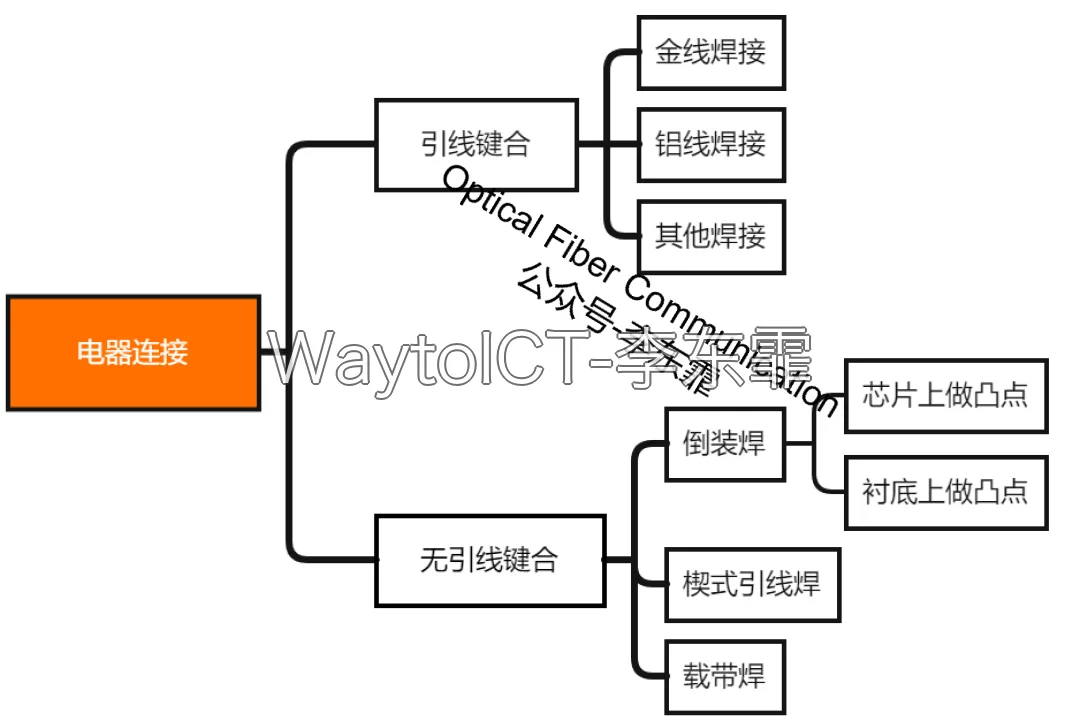
By the electrical connection method, chip interconnect can be divided into wire bonding and wire-bond-free approaches.
Wire bonding uses gold or aluminum wire to form gold-gold, gold-aluminum, or aluminum-aluminum bonds between two pads. Because these bonds are made under pressure, wire bonding is also known as thermocompression bonding.
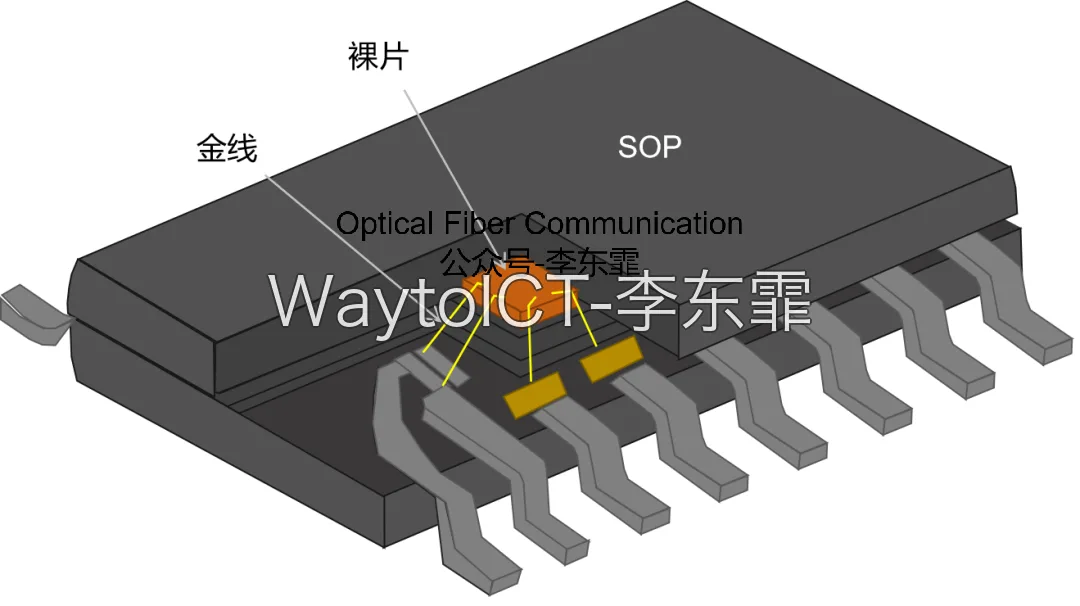
See also: Chip Packages: DIP, SOP, QFP, and LCC
In traditional chip packaging, wire bonding is mainly used to connect the pads on the die to the leads on the package base or substrate, carrying electrical signals and power.
To answer the question above: the Mitsubishi EML article does indeed use wire bonding, but its purpose is to introduce a peaking circuit, using its frequency-dependent impedance to produce a peaking effect and significantly boost modulation bandwidth.
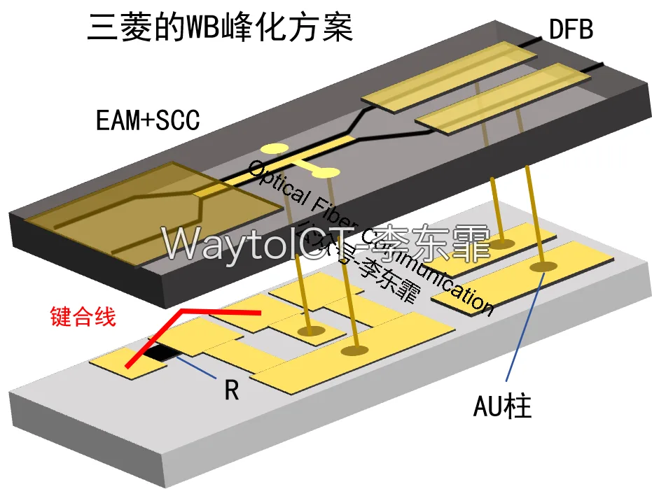
So the wire bonding in the Mitsubishi case is not the traditional wire bonding used for electrical interconnection and mechanical fixing.
Flip chip (FC), as shown in the mind map above, can be regarded as a wire-bond-free approach.
What is flip chip? Depending on whether the electrode-bearing side of the die faces up or down relative to the substrate, packages are divided into face-up and face-down (flip-chip, FC).
- Flip chip connects to the substrate or carrier through metal bumps for electrical interconnection.
- Face-up (wire bonding) connects to external circuits through bonding wires or other methods.
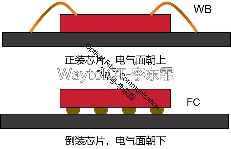
However, because wire bonding must bond multiple pads one by one, it is slow in production, and the leads must be flipped up or down, which is unfavorable for thin packaging.
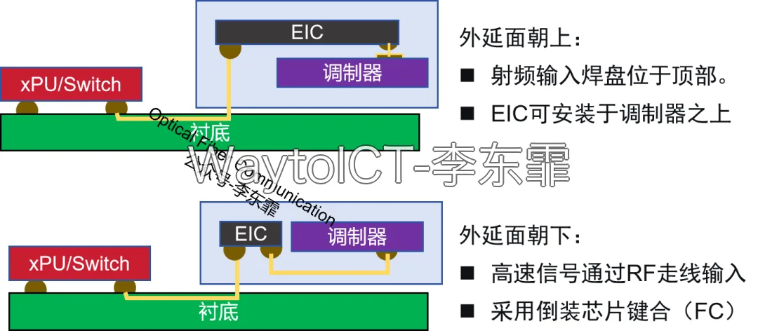
That is why many companies are developing wire-bond-free approaches, such as Mitsubishi’s two wire-bond-free solutions.
- Epitaxial-side-up design: uses on-chip integrated resistors and direct probing, achieving 85 GHz bandwidth on an AlN/glass hybrid substrate.
- Epitaxial-side-down design: achieves pure flip-chip FC interconnect through electrode planarization, fundamentally removing bond-wire inductance, with a simulated bandwidth of 145 GHz.
Thanks for reading!
Enjoy this article?
Subscribe to get new optical communication insights delivered to your inbox. Free, unsubscribe anytime.