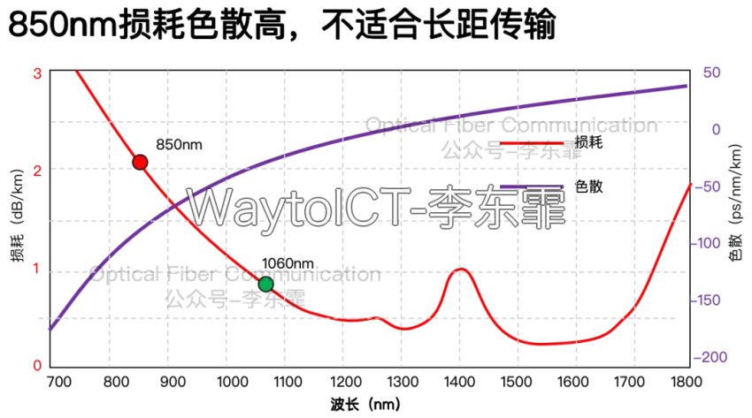
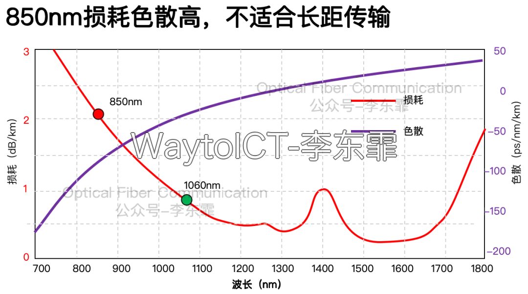
850 nm has long been the mainstream wavelength for data-center VCSELs, but it suffers from relatively high loss in long-reach multimode fiber.
In Scale-Up scenarios, especially along the Wide-and-Slow route, NPO/CPO designers would very much like VCSELs to be arrayed.
Conventional top-emitting VCSELs can be arrayed through wire bonding, but their channel count is small, the bond wires introduce noticeable parasitic inductance, and the optical path and electrodes are prone to mutual interference.
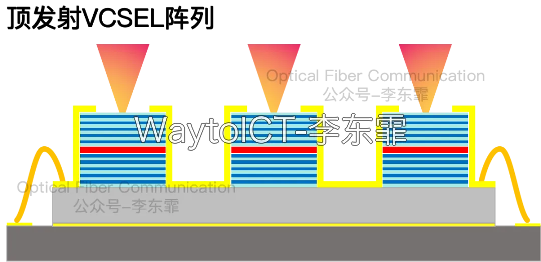
When the active region faces upward, heat has to travel through the relatively thick GaAs substrate before reaching the heat sink, so thermal dissipation is also less than ideal. For this reason, NPO/CPO leans toward flip-chip VCSELs, which in turn require back-side emission.
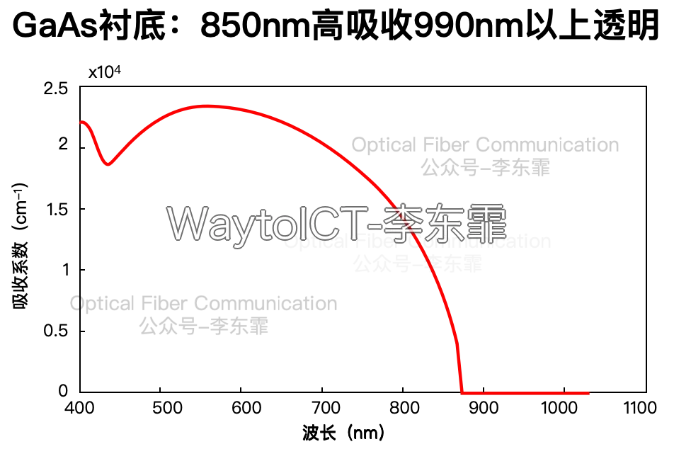
Moreover, GaAs is opaque to 850 nm, so building a flip-chip back-emitting VCSEL requires either changing the substrate or changing the wavelength.
If the substrate is switched to transparent sapphire or GaP, the 850 nm band can pass through GaP to realize bottom-emitting arrays, but the long-reach transmission limitation remains.
For the wavelength-switching approach, some vendors choose 990-1065 nm, which is longer than the GaAs absorption edge, making the GaAs substrate essentially transparent and thus enabling substrate-side emission.
Coherent’s approach uses 1060 nm to realize a back-emitting array, with a GaAs lens monolithically integrated on the back side.
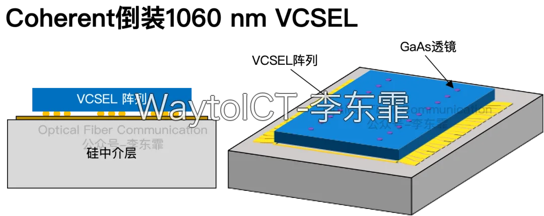
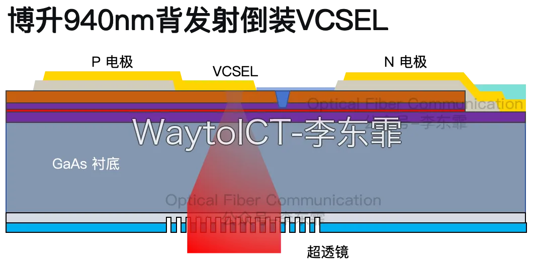
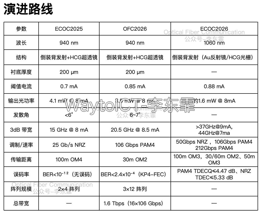
Bosheng follows a similar path: in 2025 it moved from 850 nm to 940 nm, adopting a back-emitting structure at 25 Gbps NRZ.
See also: Bosheng: Metalens Scheme Integrated on the Backside of VCSEL/PD
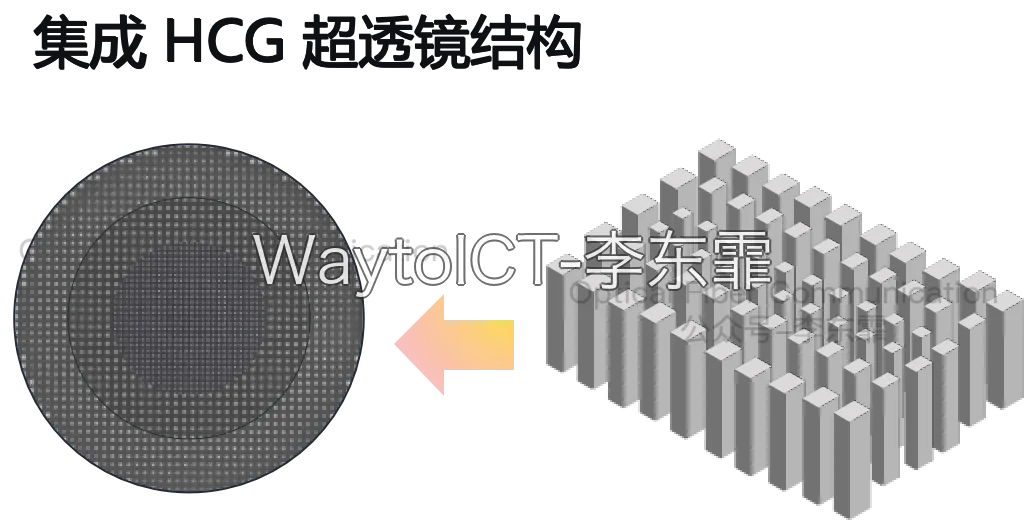
At the same time, a high-contrast-grating (HCG) metalens is monolithically integrated on the chip back side for beam collimation and focusing, compressing the far-field divergence angle and enlarging the fiber-coupling tolerance.
By OFC 2026, Bosheng’s scheme was still at 940 nm, but the data rate jumped from 25 Gbps NRZ to 106 Gbps PAM4.
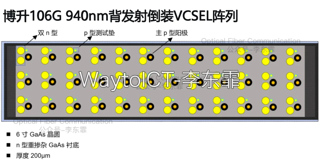
The array grew from the previous year’s 2×4 to 3×12, totaling 36 VCSEL units for NPO integration, of which 16 channels are selected to realize a 1.6T VCSEL array.
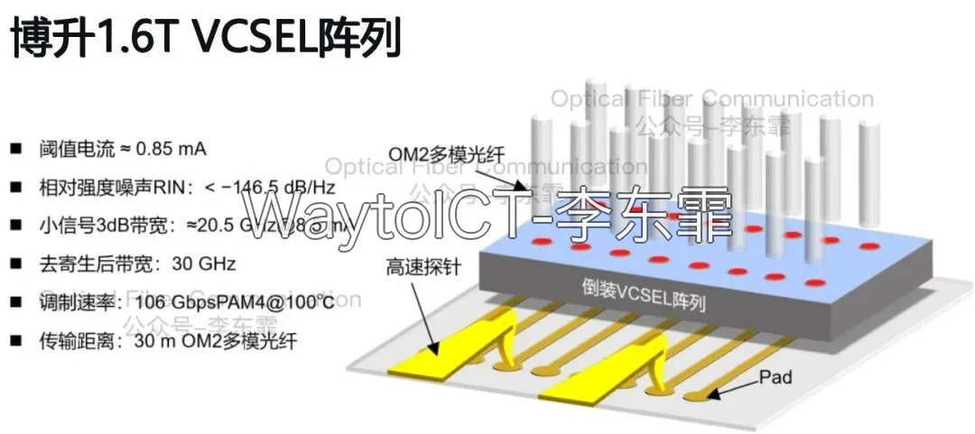
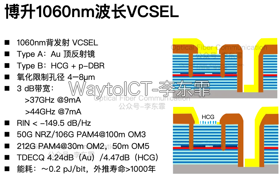
By ECOC 2026, Bosheng switched the wavelength to 1060 nm and designed two different mirror structures: an Au gold-mirror VCSEL and an HCG grating-mirror VCSEL.
Judging from the figure, the two structures share essentially the same active region, oxide aperture, and electrode layout; both make front-side electrical contact and emit from the back side after substrate thinning and polishing, differing only in the top mirror.
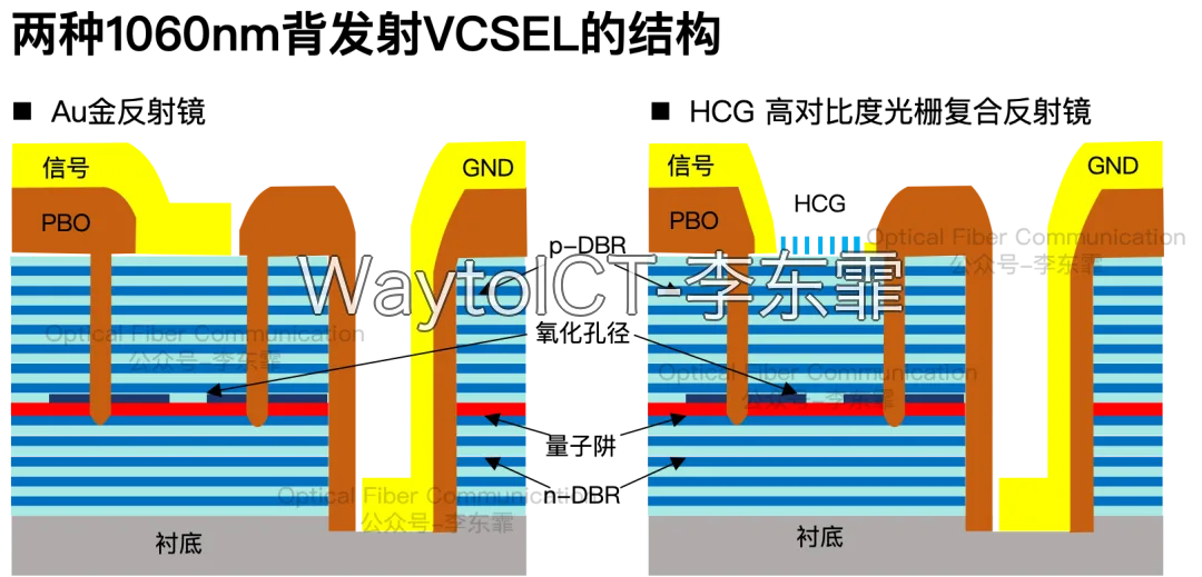
The difference lies in the front mirror: the gold-mirror VCSEL uses gold as part of the top mirror, while the HCG grating-mirror VCSEL combines the HCG with a p-DBR to provide polarization selectivity.
The HCG grating is integrated on top of the cavity, i.e., on the p-side / chip front side, acting as a reflective intra-cavity grating that reflects light and locks the polarization, achieving a polarization extinction ratio of 13.4 dB at 6 mA.
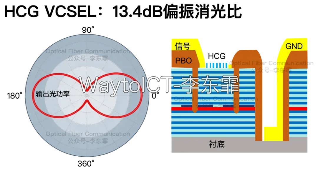
See also: High-Contrast Gratings and Multimode/Singlemode VCSELs
Using a gold film keeps the process simple, avoiding the complex HCG grating and favoring volume production. Note that the HCG here does not perform beam shaping – it is different from the HCG metalens shown at ECOC 2025 / OFC 2026.
To reduce RF parasitics, the GSG pads are made as tapered coplanar-waveguide electrodes for high-frequency probe testing, with all pads placed on benzocyclobutene (PBO).
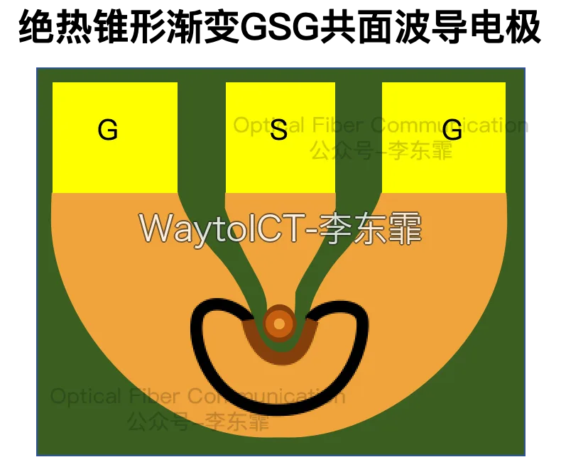
Here, the n-contact metal is routed onto the PBO surface on the epitaxial side, then electroplated with thick metal to reduce resistance and RF loss.
The CPW characteristic impedance from the pad to the VCSEL is tapered adiabatically from 50 ohm to 100 ohm to improve impedance matching with the VCSEL.
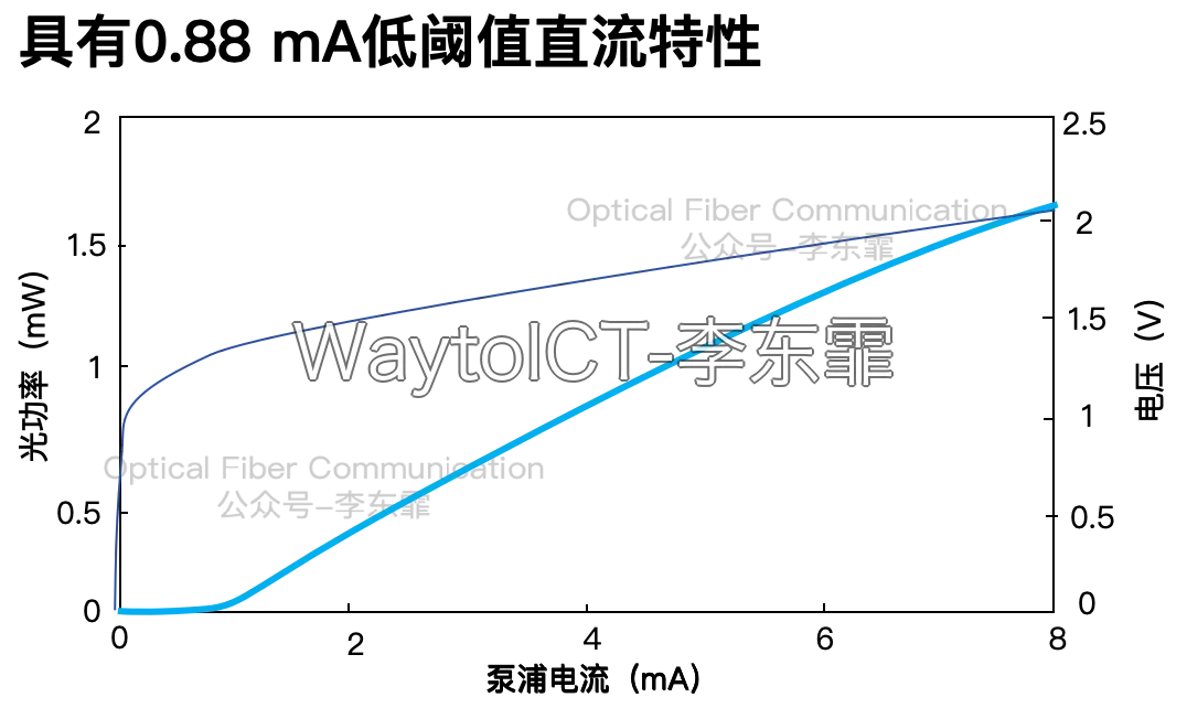
Bosheng’s typical 1060 nm VCSEL device shows a threshold current of about 0.88 mA and a differential resistance of 101 ohm at 8 mA.
Both VCSELs exceed 37 GHz of 3 dB modulation bandwidth at 9 mA bias, and both achieve 50 Gbps NRZ and 106 Gbps PAM4 transmission over 100 m OM3 fiber.
In addition, in Bosheng’s external reports and ECOC live demos in July and September this year, it mentioned achieving 43.97/44 GHz bandwidth at 7 mA, supporting 212 Gbps PAM4 transmission.
Finally, a review of Bosheng’s VCSEL scheme evolution over the past two years.
Thanks for reading!
Enjoy this article?
Subscribe to get new optical communication insights delivered to your inbox. Free, unsubscribe anytime.