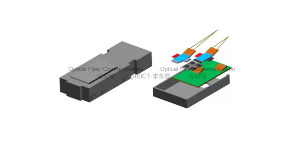
This article is part of the WaytoICT paid reading column. The technical analysis and accompanying schematics require a ¥9.9 payment to unlock! Next, let’s look at how Eoptolink implements the 6.4Tbps high-bandwidth engine packaging in its silicon photonics scheme. The transmitter uses silicon photonics integration technology with a single-channel rate of 200Gbps. Each silicon photonics…
Technology
Tencent: 3.2T NPO Technology Evolution and Scale-Out/Scale-Up Roadmap
This article is part of the WaytoICT paid reading column. The technical analysis and accompanying schematics require a ¥9.9 payment to unlock! Looking further at Scale-Up networks, there are mainly two forms: centralized nodes and distributed nodes. A centralized example is NVL72, which relies on copper-cable interconnection within the chassis for low cost, but is…
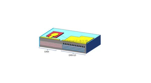
Anti-Reflection Structures and Schemes for High-Speed EML Lasers
This article is part of the WaytoICT paid reading column. The technical analysis and accompanying schematics require a ¥9.9 payment to unlock! In practice, many manufacturers combine the window structure with the angled output waveguide. For example, Huawei’s EML chip for PON applications in 2023 adopted both designs simultaneously. In 2025, Source Photonics also introduced…
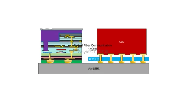
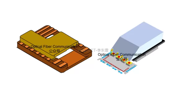
TSMC: CPO Packaging Flow Based on Silicon Photonics TDV Process
This is a WaytoICT paid-reading column. The full technical analysis and accompanying schematics require a ¥9.9 payment to unlock! The top pads are used to interface with the EIC chip, and BGA solder balls are fabricated on the bottom for connection to the PCB. It can also be connected to a silicon interposer through microbumps…