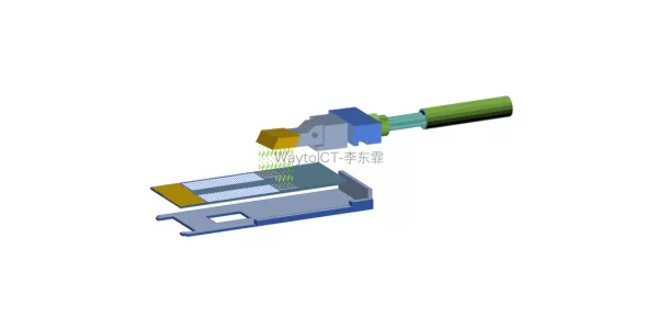
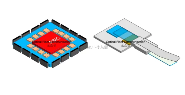
This is a WaytoICT paid-reading column. The full technical analysis and accompanying schematics require a ¥9.9 payment to unlock! Generally, the diffusion hole needs to enclose the entire P ohmic contact ring. On the chip surface, the region enclosed by the inner diameter of the P ohmic contact ring is defined as the photosensitive area…
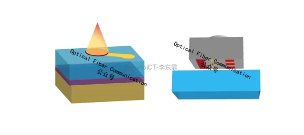
Technology
Ge Electro-absorption Modulator
If you are interested in semiconductors / chips / optical components & modules / optical fiber communications Welcome to follow us! In a modulator, the basic idea behind changing light intensity is to rely on the interference of two light beams – when the interference is constructive, it is “1”, and when destructive, it is…
The e-Tube Plastic Waveguide Solution Supporting CPO
This is a WaytoICT paid-reading column. The full technical analysis and accompanying schematics require a ¥9.9 payment to unlock! Its working principle is actually a process of “electrical to RF, then RF back to electrical.” At the transmitting end, the digital signal is fed into a millimeter-wave RF SoC chip and modulated onto a very…
Glass Substrate: Pluggable Connection Scheme in CPO Packaging
This article is part of the WaytoICT paid reading column. The technical analysis and accompanying schematics require a ¥9.9 payment to unlock! The main component of glass is silica, the same as optical fiber. Because the materials are similar, waveguides made from it match the dimensions of optical fiber, resulting in very low coupling loss….