Skip to content

WaytoICT

通往ICT之路 · 光通信与AI网络技术解读

中文English
登录注册
Menu
Technology Optical comms · silicon photonics · CPO → Market Insights Financials · trends · industry → In-Depth Analysis Optical chips, devices & modules → Video Understand a topic in minutes → Documents Latest docs · summit materials →
Menu

Technology

1.6T/3.2T Optical Modules: Half-DSP, Half-LPO Hybrid Architecture

Posted on 2026-01-15 by

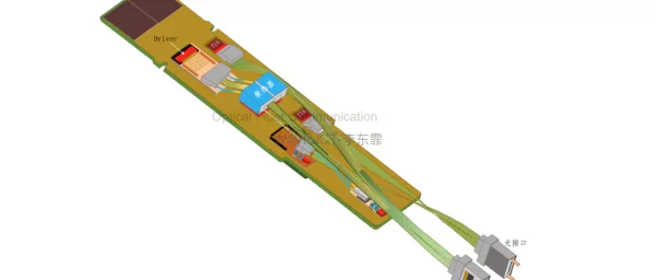
This is a WaytoICT paid-reading column. The full technical analysis and accompanying schematics require a ¥9.9 payment to unlock! Another is the LPO scheme, which the industry currently also regards as a transitional scheme for optical modules at 800G and above in short-distance transmission. LPO completely abandons DSP; power consumption is lower, but the requirements…
Read more

Eoptolink: VCSEL-Based NPO Optical Engine

Posted on 2026-01-12 by

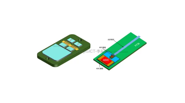
This article is part of the WaytoICT paid reading column. The technical analysis and accompanying schematics require a ¥9.9 payment to unlock! The VCSELs and photodetectors are mounted together, in an array, on a large copper heat-spreading layer. They are connected to the substrate pads via gold wires. The detectors are flip-chip mounted with their…

Read more

Quantum Wells and Quantum Dots: Innolume’s High-Power CPO Quantum Dot Laser

Posted on 2026-01-12 by

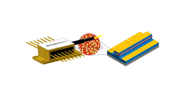
This article is part of the WaytoICT paid reading column. The technical analysis and accompanying schematics require a ¥9.9 payment to unlock! In 2023, Innolume’s O-band quantum dot DFB laser demonstrated excellent temperature stability, so the TEC can be removed to reduce cost and power consumption. It remains highly efficient at 125°C, with an output…

Read more

Google: Next-Generation Optical Switching Technology

Posted on 2026-01-07 by

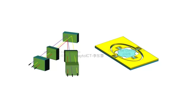
This article is part of the WaytoICT paid reading column. The technical analysis and accompanying schematics require a ¥9.9 payment to unlock! Its core uses deep reactive ion etching to fabricate large-area, high-flatness, high-reflectivity micromirrors on a silicon wafer. In terms of process, it is achieved by etching suspended beams and precise comb structures on…

Read more
  • Previous
  • 1
  • …
  • 19
  • 20
  • 21
  • 22
  • 23
  • 24
  • 25
  • …
  • 73
  • Next

订阅更新

订阅后,新文章发布时第一时间收到邮件通知

李东霏
光互连技术研究者

香农信息技术研究院,专注光模块、CPO、硅光与 AI 光互连的技术解读。

行业报告

光芯片·光器件·光模块 2026 报告汇编(含 OFC 2026)

光芯片 · 光器件 · 光模块
2026 报告汇编(含 OFC 2026)

¥1,900

上/下两册,收录 OFC 2026 一线报告
添加微信 WaytoICT 订购

广告

📢 广告位招商:面向全球光通信客户 侧边栏广告位 Email:Dongfei.li@shannoninstitute.cn

最新文档

  • 互连拐点:11 页解析机架内到多机架 Scale-Up 的 XPO/CPX/OCI 蓝图(OCP 2026 全球峰会)
  • AI 时代的相干光技术:17 页解析 Scale-Across、液冷 XPO 与全谱转发器(OCP 2026 全球峰会)
  • XPO 高密度光互连的系统级评估:20 页解析 212G SerDes 平台与 FRO/LRO/LPO 实测(OCP 2026 全球峰会)
  • CPO 与 OCI 标准及未来技术:17 页 Broadcom 精简版演讲提纲(OCP 2026 全球峰会)
  • VCSEL 高密度互连:7 页解析 50G NRZ「慢而宽」阵列与光 PCIe 演示(OCP 2026 全球峰会)

最新评论

暂无评论,欢迎登录后发表第一条评论。

最近访客

👥 今日访客 -
加载中…
© 2026 WaytoICT | 蜀ICP备2020035321号-2 | 隐私政策 | 免责声明
Wechat Pay
Alipay
请使用 支付宝 或 微信 扫码支付