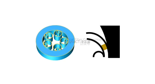
This article is part of the WaytoICT paid reading column. The technical analysis and accompanying schematics require a ¥9.9 payment to unlock! So, what is a node? This leads to the distinction within DNANF: fibers that successfully achieve or come very close to the ideal “nodeless” structure during fabrication are called standard DNANF (S-DNANF). Fibers…
Photosensitive Area: From Principles to 200G/Lane Back-Illuminated and Flip-Chip
This is a WaytoICT paid-reading column. The full technical analysis and accompanying schematics require a ¥9.9 payment to unlock! Generally, the diffusion hole needs to enclose the entire P ohmic contact ring. On the chip surface, the region enclosed by the inner diameter of the P ohmic contact ring is defined as the photosensitive area…
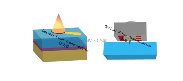
Ge Electro-absorption Modulator
If you are interested in semiconductors / chips / optical components & modules / optical fiber communications Welcome to follow us! In a modulator, the basic idea behind changing light intensity is to rely on the interference of two light beams – when the interference is constructive, it is “1”, and when destructive, it is…
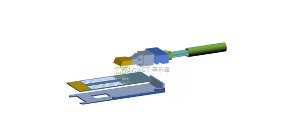
The e-Tube Plastic Waveguide Solution Supporting CPO
This is a WaytoICT paid-reading column. The full technical analysis and accompanying schematics require a ¥9.9 payment to unlock! Its working principle is actually a process of “electrical to RF, then RF back to electrical.” At the transmitting end, the digital signal is fed into a millimeter-wave RF SoC chip and modulated onto a very…