Let’s start with a brief introduction to the Open CPX MSA.
It is an international industry alliance whose founding members are Ciena, Coherent, Marvell, Molex, Samtec, and TeraHop. The goal of the alliance is to unify the mechanical structure and performance specifications of optical engines and promote their large-scale adoption.

Here, CPX stands for Co-packaged Interface, targeting CPO and NPO scenarios. The Open CPX MSA V1.0 specification was officially released on September 16, 2026.
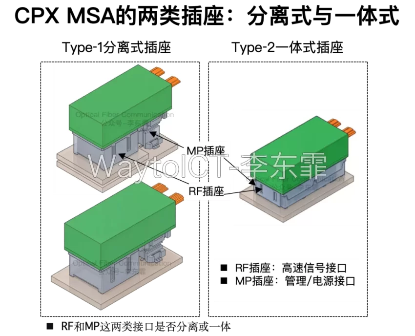
The specification defines two CPX hardware architectures: the split-socket Type-1 and the integrated-socket Type-2.
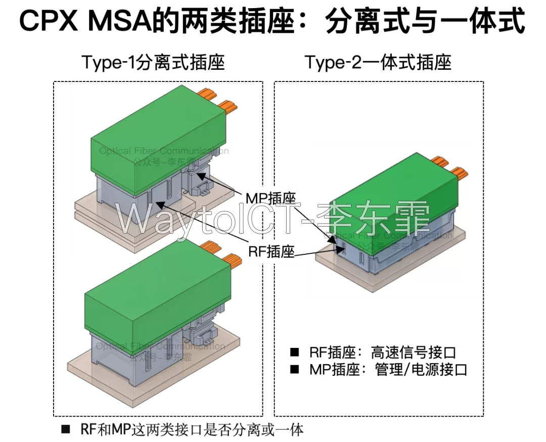
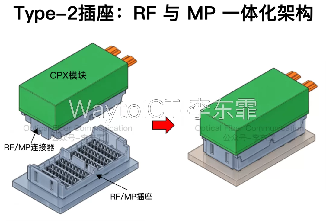
The two CPX module types are essentially identical in form factor. Type-1 consists of two independent sockets, RF and MP; Type-2 merges them into a single RF/MP socket, which is larger but more highly integrated, eliminating the separate MP socket.
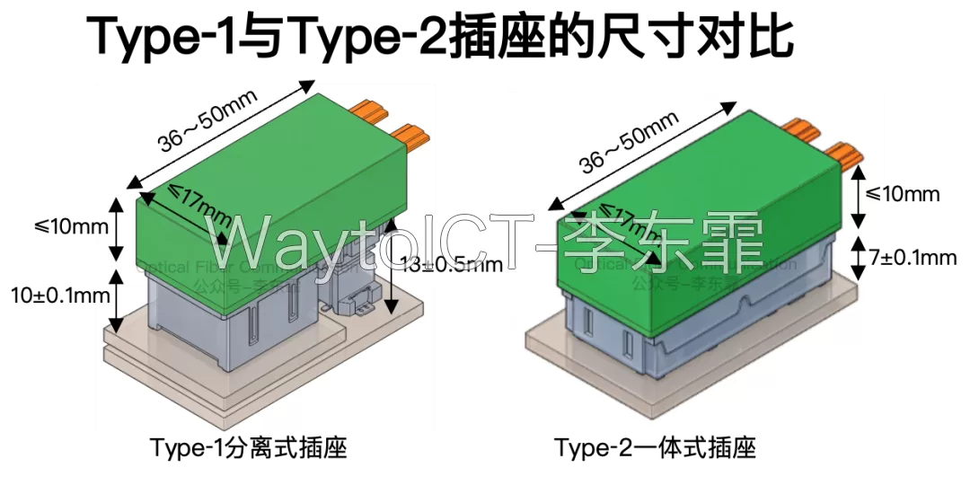
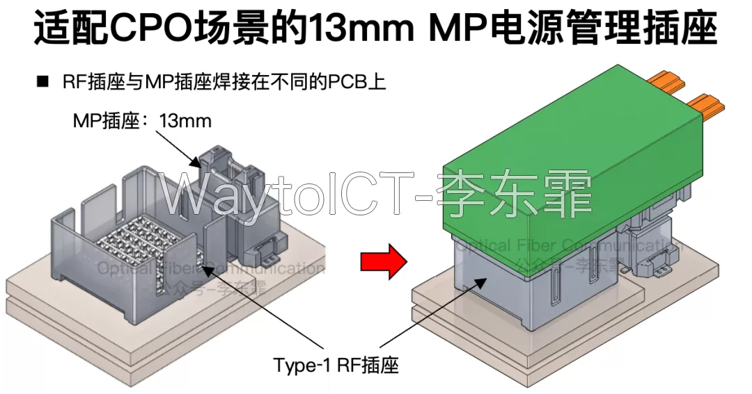
In addition, the Type-1 socket has two independent parts: the RF high-speed signal socket and the MP management/power socket. Typically, the RF socket is soldered onto the ASIC package substrate, while the MP socket is soldered onto the motherboard.
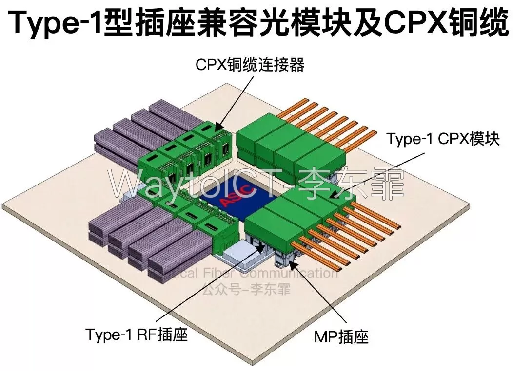
Because the RF and MP are physically separate, they can be mounted on different mounting planes.
If the RF is soldered to the ASIC package substrate and the MP to the motherboard, there is a height difference of about 3 mm between them; this corresponds to the CPO co-packaged scenario, which uses a 13 mm MP socket.
If the RF and MP are on the same plane, for example in the NPO scenario where the RF socket is soldered onto the PCB and the MP socket is also soldered onto the same PCB, the MP socket is 10 mm high.
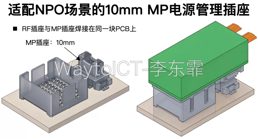
It is worth noting that 10 mm corresponds to RF/MP coplanar mounting, while 13 mm corresponds to offset mounting where the MP is about 3 mm lower than the RF. NPO/CPO are only typical application scenarios, not mandatory correspondences.
The Type-2 CPX socket, by contrast, targets single-board, high-density, NPO near-package interconnect and is an integrated socket.
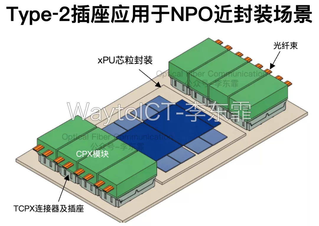
Unlike the Type-1 split of RF socket plus MP socket, the Type-2 combines the high-speed RF and the management/power MP into the same socket and the same pin area.
However, the current V1.0 defines the Type-1 and Type-2 optical modules; the copper-cable solution is outside the scope of this specification.
The Type-2 socket contains a total of 12 rows of contacts, with 25 positions per row; it uses a differential-pair arrangement with ground contacts added between rows to suppress crosstalk; it supports up to 36 high-speed channels, or 72 differential lanes, with each channel supporting up to 212.5 Gb/s PAM4.
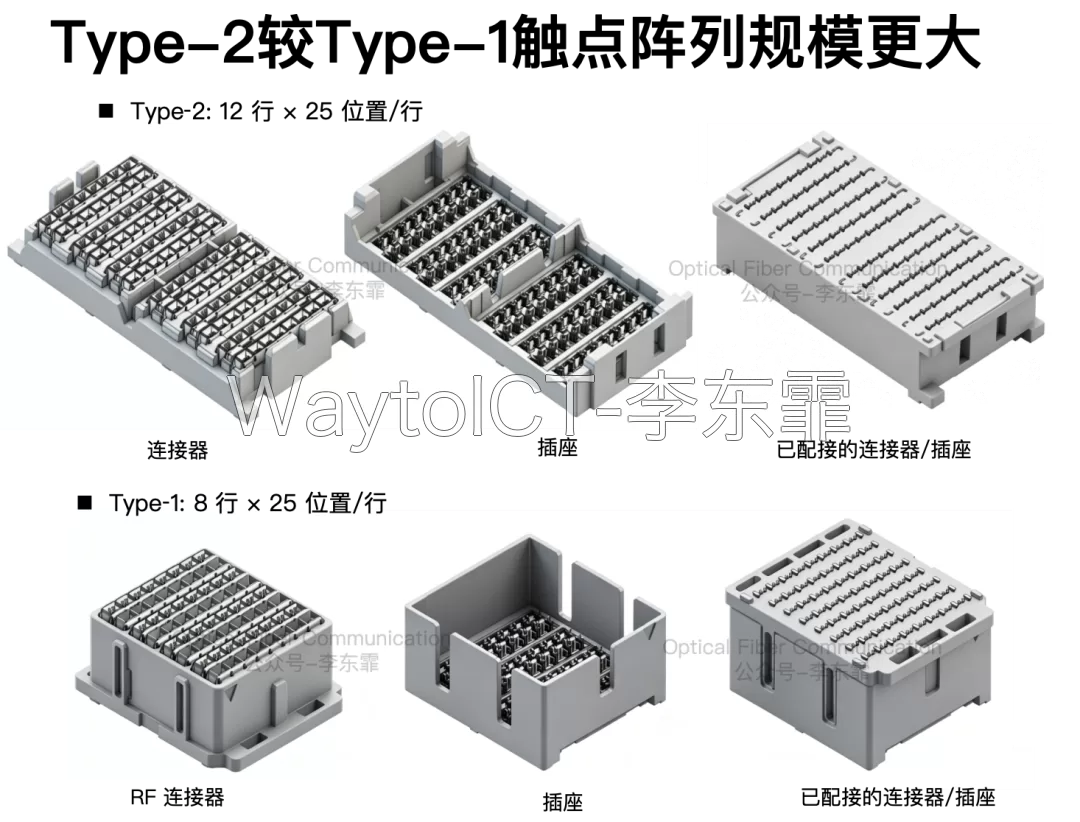
The Type-1 also supports up to 212.5 Gb/s PAM4 per channel, but with fewer total channels than the Type-2.
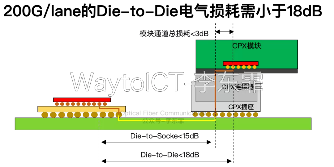
For the 212.5 Gb/s rate running at 106.25 GBd PAM4, the specification allows a Die-to-Die loss of less than 18 dB, of which the Die-to-socket loss is less than 15 dB.
For the light source, Open CPX supports both external laser (ELM + ELS/ELSFP) and internal laser (ILM) solutions.
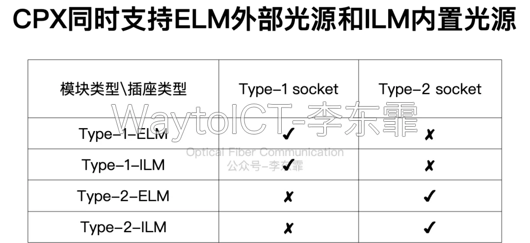
ELM requires external laser fiber and an additional ELS management interface, and is suitable for centralized laser, centralized cooling, and redundant architectures; ILM integrates the laser inside the module, simplifying fiber routing but placing greater thermal and power pressure on the module.
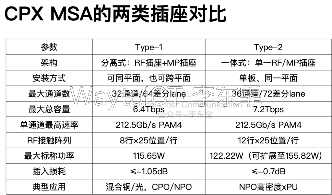
Finally, let’s briefly compare the two socket types.
Thank you for reading.
Please forgive any inaccuracies!
The Optical Chips, Optical Components, and Optical Modules (OFC2026) report compilation is printed in color and A4-bound in two volumes totaling about 525 pages and roughly 200,000 words. Contact us to order – the price is affordable!
Related Reading
- Scale Up: Is It PLO, NPO, or CPO?
- Pluggable, OBO, NPO and CPO
- Murata: NPO/CPO Technology and Evolution Roadmap Based on Low-Temperature Co-fired Ceramic
Enjoy this article?
Subscribe to get new optical communication insights delivered to your inbox. Free, unsubscribe anytime.