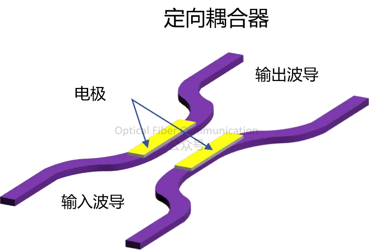
A reader privately messaged asking me to explain multi-mode interferometers and directional couplers, probably after reading yesterday’s article Samsung: Latest Performance and Evolution Roadmap of the CPO Silicon Photonics Platform.
Let’s start with directional couplers and related devices.
A directional coupler is easy to understand. Two physically separate single waveguides, each supporting an independent guided mode.
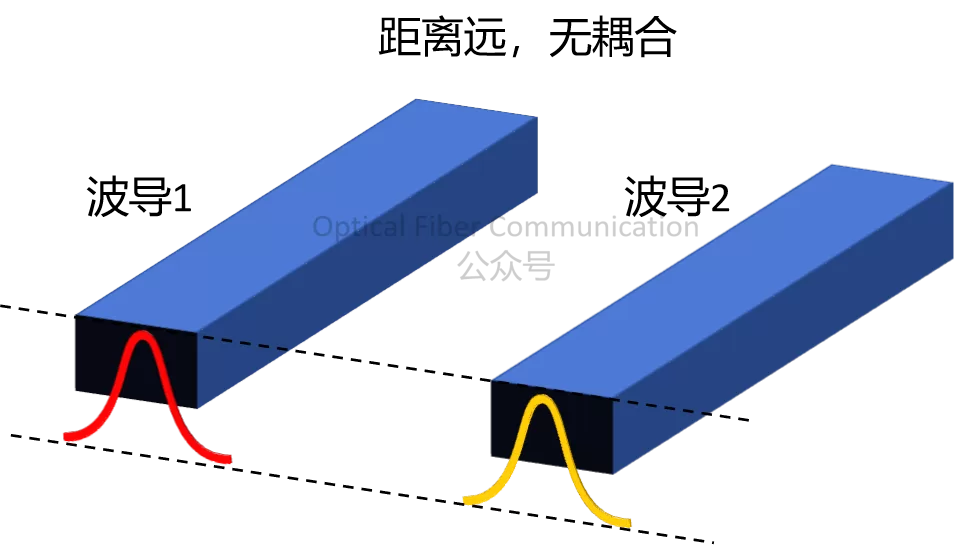
When the spacing between the two waveguides is large enough, the evanescent fields barely overlap, the modes are completely independent, and there is no energy coupling.
When the two waveguides are close enough, the evanescent fields of the guided modes overlap, and optical power is periodically exchanged between the two waveguides.

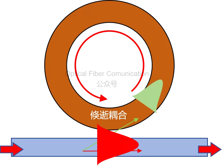
If we replace one straight waveguide with a ring-shaped closed waveguide, we actually form a microring structure.
HiSilicon / Intel: SiN-SOI Microring Modulators for CPO
Evanescent Waves and Evanescent Coupling
Silicon Photonics Coupling: Wedge and Slot SSC Mode-Spot Converters
The upper and lower coupling regions of the microring are essentially two back-to-back directional couplers. However, unlike straight-waveguide coupling, the microring introduces a resonance effect, so it can achieve wavelength-selective coupling.
Continuing with the two straight-waveguide coupling we just discussed. When the propagation constant difference of the two newly generated modes is zero, complete energy exchange occurs; otherwise only partial energy exchange occurs.
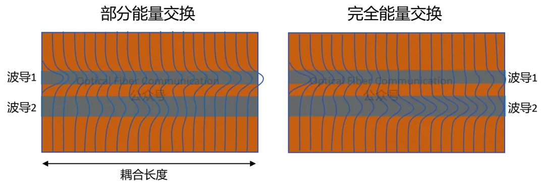
By controlling the coupling length, couplers with any splitting ratio can be designed in theory, such as 10:90, 50:50, 20:80, 70:30, and so on.
We can also add electrodes to the two strip waveguides and inject current to change the refractive index of the waveguide arms, thereby creating a difference in propagation constant between the two waveguides and achieving coupling at different ratios.

It should be noted, however, that light cannot be transmitted 100% perfectly during coupling, transmission, and abrupt structural changes; absorption, scattering, leakage, and reflection will inevitably occur, all of which introduce loss.
For example, in yesterday’s article we mentioned that the insertion loss of the silicon and silicon nitride directional couplers on Samsung’s platform is less than 0.1 dB.

Samsung: Latest Performance and Evolution Roadmap of the CPO Silicon Photonics Platform
In extreme cases, the directional coupler operates in two output states of 0% and 100%, and can switch between the two states, at which point it realizes the function of an optical switch.
As shown below, an optical switch is realized by directly electrically controlling the directional coupler.
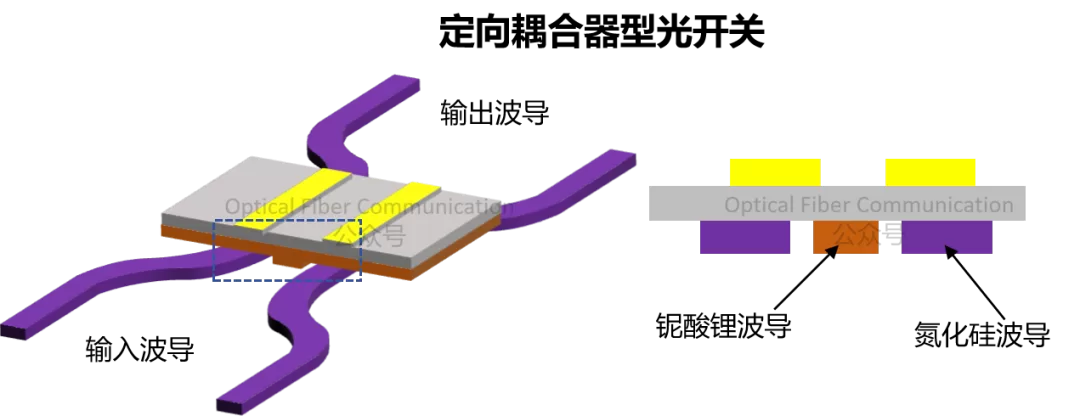
Among them, the SiN waveguide is responsible for low-loss, long-distance optical transmission, while the tunable waveguide made of lithium niobate is responsible for high-speed electro-optic control.
In addition, relying on the splitting and combining functions of directional couplers, Mach-Zehnder optical switches can also be realized.
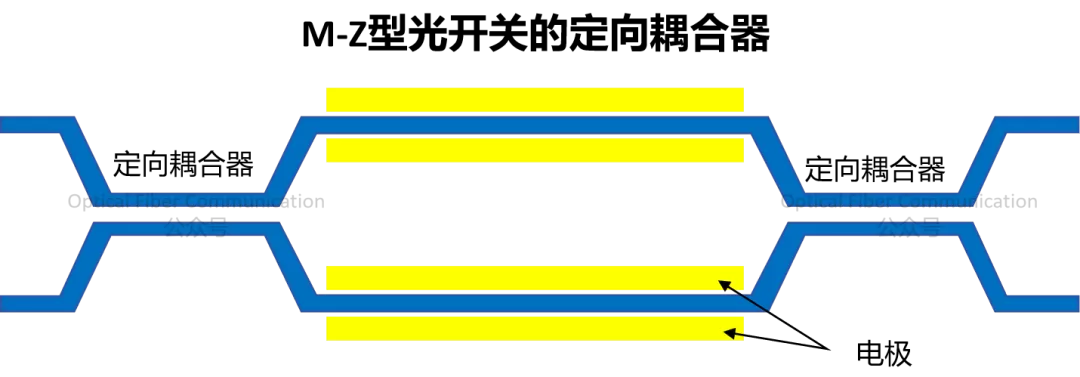
ZTE: Mach-Zehnder Modulators and CPO White-Box Switches
Thanks for reading!
Add WeChat WaytoICT to join the Semiconductor & Optical Component Industry Chain Group 2.
Welcome to join our community and access high-value technical documents, trend research reports, and various supply-demand business opportunities in the fields of semiconductor chips, optical components, and optical modules.

If you are interested in semiconductors / optical components / optical modules / optical fiber communications
Welcome to follow us!
Related Reading
- Maximum Coupling Loss (MCL) and Maximum Path Loss (MPL)
- How to Couple VCSEL Light into the PIC Wafer Plane?
- Silicon Photonics Series 2: What Is a Grating Coupler?
Enjoy this article?
Subscribe to get new optical communication insights delivered to your inbox. Free, unsubscribe anytime.