Dry etching is an etching process carried out under atmospheric or vacuum conditions, usually using ions or chemical substances in a gas to remove part of the material surface. Through the regulation of the mask and etching parameters, it can switch arbitrarily between anisotropic and isotropic etching, thereby forming the desired pattern or structure. Common dry-etching equipment includes reactive ion etchers (RIE), inductively coupled plasma etchers (ICP), magnetic neutral line plasma etchers (NLD), and ion beam etchers (IBE). The purpose of this article is to analyze the structure of each etching equipment and the advantages and disadvantages of each technology.
RIE
The structure of RIE equipment is usually relatively simple, generally composed of an RF power supply, anode, cathode, gas source, and vacuum pump. The wafer is placed on the cathode, and the RF power supply is connected to the cathode. At the start of etching, the RF power supply applies an electric field to the gas, which is ionized into ions, electrons, atoms, and molecules. Because electrons move much faster than other ions, an obvious sheath region forms in the etching chamber, and a self-bias electric field forms above the wafer. RIE uses this effect to attract and accelerate the ions in the plasma to produce physicochemical interaction with the material being etched, and the resulting byproduct gas finally volatilizes and is discharged. However, the different movement speeds of the various substances during the etching process caused by this self-bias effect result in a mismatch between RIE etching ions and reactive free radicals. The “black silicon” phenomenon that often occurs during RIE etching is caused by this principle.
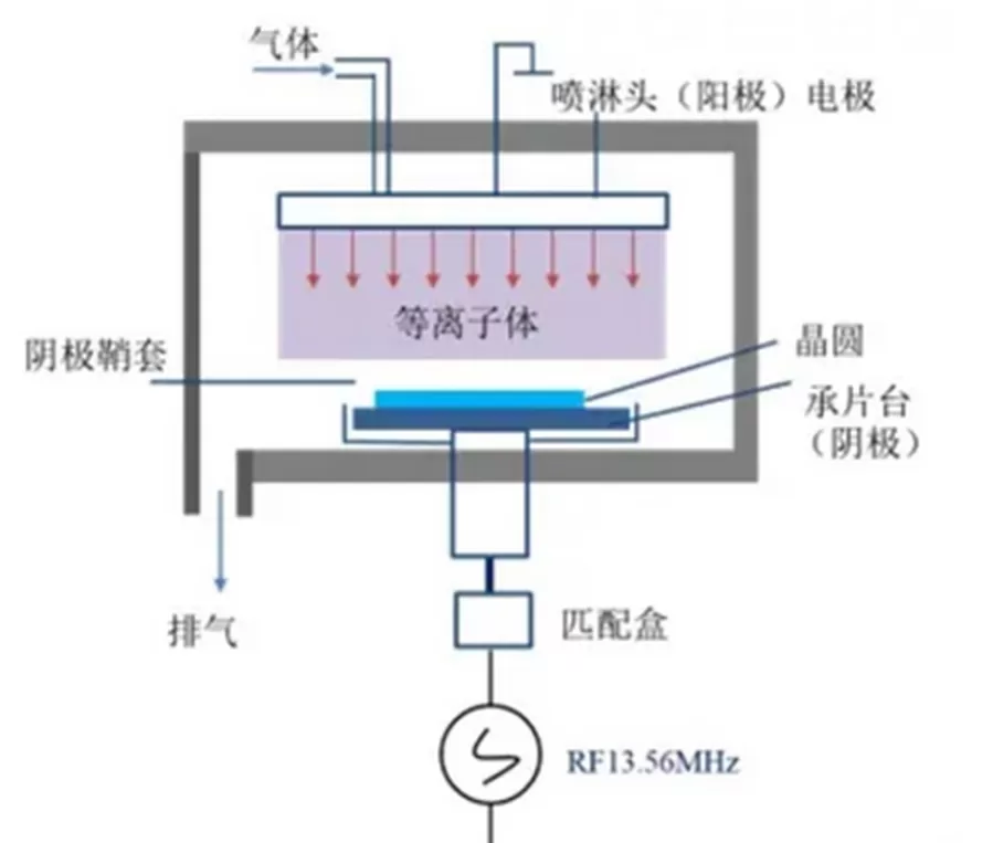
Figure 1: Schematic of RIE etching structure
ICP
As process requirements continued to improve, researchers developed the inductively coupled plasma etcher (ICP), which overcame the problem of free-radical and ion mismatch. The structure of a commonly used ICP etcher is shown in Figure 2. Etching gas is generally introduced from the top, passes through the RF coil on the sidewall of the etching chamber, and is excited into a plasma by the electric field applied by the RF coil, forming an obvious glow layer in the chamber; then, the etching ions in the plasma are absorbed by applying a bias power on the lower electrode. Compared with RIE etching technology, the ICP etching chamber generally has lower pressure and higher plasma density, and can achieve higher rate, higher precision, and larger aspect-ratio etching through the regulation of RF coil power, gas flow rate, and bias power.
The right side of Figure 2 shows the process of ICP etching quartz using C4F8. The fluorocarbon free radicals produced by the RF discharge of C4F8 spontaneously form a passivation layer deposited on the surface. Then, under the bias applied on the wafer surface, positive ions bombard the passivation layer and etch the quartz at a high rate perpendicular to the wafer surface, achieving high-aspect-ratio etching of quartz.
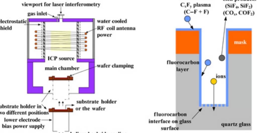
Figure 2: Composition of ICP etcher and etching example
NLD
The RF coil of traditional ICP etching affects the magnetic field in the etching chamber, making the radial plasma density inconsistent and interfering with the movement of etching ions, thus affecting etching uniformity. Researchers further developed magnetic neutral line discharge, whose structure is shown in Figure 3. Three magnetic-field-control coils are applied around the ICP etching coil. By controlling the magnetic-field magnitude of the three coils, an environment with a magnetic neutral loop intensity of 0 can be formed in the etching chamber, thereby producing plasma with higher density and uniform distribution. With bias control, NLD technology has better etching uniformity and higher etching rate. In addition to common dielectric layers, it is also often used to etch etch-resistant materials such as silicon carbide.
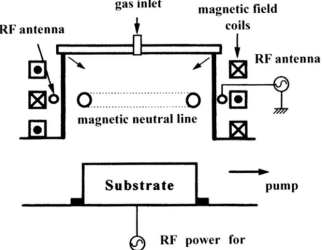
Figure 3: Structure of NLD etcher
IBE
IBE etching is pure physical-bombardment etching, often used for materials that cannot be etched by fluorine-based or chlorine-based plasma, such as gold, copper, and platinum. The structure of a conventional IBE etcher is shown in Figure 4. Argon gas is ionized into a plasma and an ion source by the electrons provided by the filament, and then the ions are directed uniformly onto the wafer worktable through the electron-extraction acceleration system, finally bombarding the solid-surface atoms to sputter the material atoms and achieve the etching purpose.
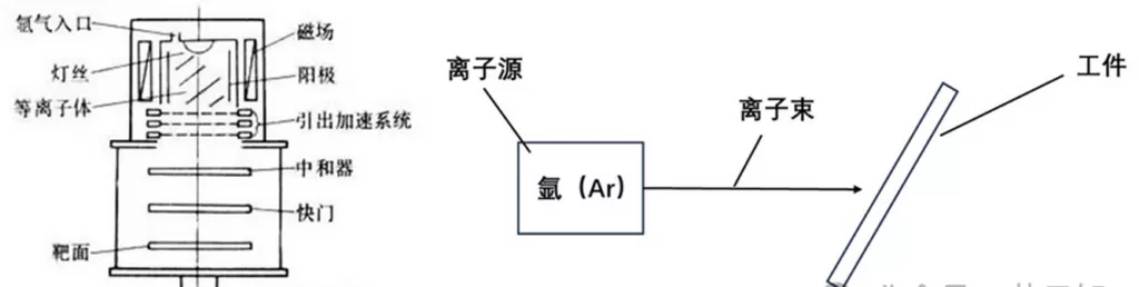
Figure 4: IBE etching structure and ion beam path
The main characteristics of IBE are: 1) The highly directional neutral ion beam can control the sidewall profile and optimize the radial uniformity and structural morphology during etching. 2) By adjusting the angle of the worktable, the wafer can be tilted to change the impact direction of the ion beam, thereby achieving control of the sidewall angle.
Related Reading
- How Does RIE Achieve Vertical Etching?
- What Is Strained-Layer Epitaxy?
- What Is the Difference Between a Semiconductor Substrate and an Epitaxial Layer?
Enjoy this article?
Subscribe to get new optical communication insights delivered to your inbox. Free, unsubscribe anytime.