
What is an ASIC chip?
ASIC, the full name of which is Application Specific Integrated Circuit, is, as the name suggests, a chip designed for a specific purpose or algorithm. The architecture of an ASIC chip is not fixed; it ranges from relatively simple network-interface-card chips used to control network traffic and meet firewall requirements, to top-tier AI chips such as Google’s TPU and the Ascend 910B. ASIC does not mean simplicity; rather, it means demand-oriented. Any chip specially designed for a certain type of algorithm or a certain type of user demand can be called an ASIC. Currently, ASIC chips are mainly divided into TPU, DPU, and NPU chips according to the type of computation, corresponding to different basic computing functions. TPU is the AI processor invented by Google, mainly supporting tensor computation; DPU is used for accelerated computing inside data centers; NPU corresponds to the CNN convolutional-neural-network algorithm in the previous AI boom, and was later widely integrated into the processing chips of edge devices through SoCs. From the broad chip category perspective, human chips can currently be divided into four major categories: CPU, GPU, FPGA, and ASIC:
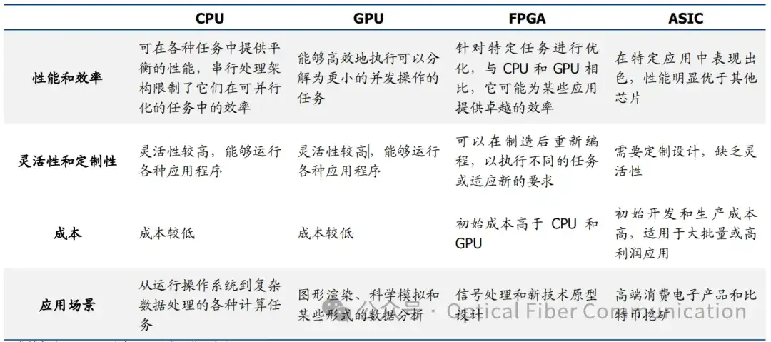
Among them, the CPU is the mother of human chips, with the strongest versatility, suitable for complex instructions and tasks. The GPU is the first major category of “ASIC” chips in human history, optimizing heterogeneous computing needs by deploying a large number of parallel computing cores. FPGA chips emphasize programmability even more; the logic gates and memory inside the chip can be reconfigured through programming, but computing performance is lower. ASIC, on the other hand, is completely specially designed for a certain type of function or algorithm, with lower versatility but the best performance for a certain type of algorithm.
The trend of chips: what is general for long becomes specialized, and what is specialized for long becomes general
From the earliest CPU dominating the world, to the rise of GPU in the parallel-computing era, to the brilliance of dedicated ASICs in the mining era, it is not difficult to find that the emergence of new chips often comes from the explosion of a certain type of demand, which separates a specific function from past general-purpose chips and forms a new chip category. General-purpose chips discover and explore demand, while dedicated chips satisfy demand. This is the semiconductor industry’s way of addressing human needs. Ultimately, demand determines everything, and whether a chip’s architecture can fit and satisfy customer needs is an important factor determining whether a chip company can succeed. In the era of large models, the wind came so fast. Before the Spring Festival of 2023, the industry was still working hard to optimize complex CNN algorithms, pursuing small and beautiful models. Later, with the emergence of GPT and OPENAI, the industry’s hot algorithms quickly shifted from CNN to Transformer, and the underlying computation also changed to matrix multiplication. At the same time, due to the “brute force creates miracles” characteristic of large models, the demand for computing power was released extremely rapidly. In 2023, the only thing that could satisfy this new user demand was still the relatively general-purpose NVIDIA chip, which created NVIDIA’s legendary $2 trillion market value within a little over a year. But among the chips of the world, what is general for long becomes specialized, and what is specialized for long becomes general. When the fixed computation of matrix multiplication occupies most of the large-model computation demand, the small cores in general-purpose chips, and even the vector computing cores, gradually become burdens on power consumption, cost, and latency. Customers ultimately will not pay extra for versatility because of a single matrix-multiplication demand. Therefore, from overseas giants to countless startups founded by industry veterans, many have joined the “matrix multiplication” ASIC, or large-model ASIC, startup wave. In the text below, we will list two relatively representative ASIC chips to look at the industry’s design thinking and evolution direction.
Development route of large-model ASICs
From a historical perspective, by dissecting the structure of the GPU and its differences from the CPU, it is not hard to find that the GPU is also an ASIC in a certain sense. Past data-processing tasks were usually single complex instructions or logic operations, but with the emergence of image-processing demand, computation often began to include a large number of parallel simple calculations. Because the CPU has a limited number of cores, although a single core can handle relatively complex instructions, its disadvantage of long computation time gradually emerged when facing large numbers of simple calculations. So, as mentioned earlier, the CPU, as the most general-purpose chip for humans, led humans into and explored the image era. Immediately afterward, facing the massive release of AI demand, the GPU emerged as an “image ASIC,” satisfying massive image-processing demand.
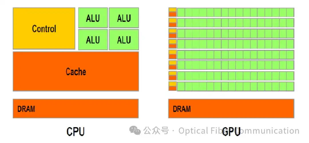
Further exploring the development history of the GPU, we discover the second part of the chip trend. If the CPU-to-GPU transition is the “what is general for long becomes specialized” we mentioned, then the development history of the GPU itself is the best illustration of “what is specialized for long becomes general.” In the early days of parallel computing, algorithms were mostly composed of simple addition, subtraction, multiplication, and division, so a large number of small cores were deployed inside the GPU chip to compute these simple algorithms in parallel. But later, as parallel computing, or image-processing demand, gradually gave rise to new functions such as image recognition, ray tracing, and machine vision, along with the corresponding new algorithms represented by “convolution computation,” the GPU itself changed from a dedicated chip into a “general-purpose chip” oriented toward parallel-computing modes or massive image demand.
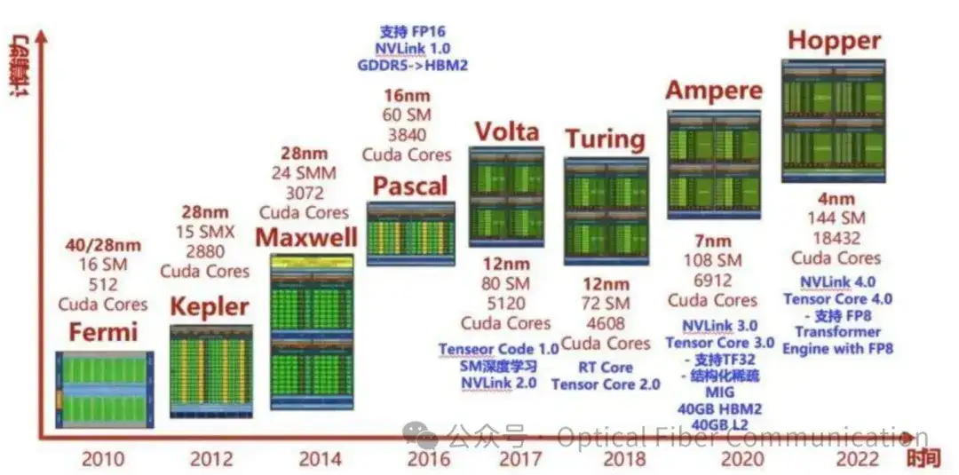
Summary of main technology trends
Looking ahead, the development of ASIC will also focus on two directions:
The first direction is “Wafer-Scaling.” Taking Cerebras, in which Sam Altman invested, as an example, this means enlarging the area of a single chip to fit more MXUs, that is, matrix-computation cores, within a single chip. In this way, a single computation can process a larger amount of data, making it the simplest and most direct upgrade route. The second direction is “near-memory computing,” concretely demonstrated by Groq. The MXU directly transfers data to the adjacent sRAM after computation. Because the transmission distance is short, combined with the inherently high bandwidth of sRAM, it achieves pipeline-style processing that bypasses HBM. We believe this model of high-speed communication between computing units through high-speed storage near the computing units will be another main direction of large-model ASIC development.
Related Reading
- How to Couple VCSEL Light into the PIC Wafer Plane?
- What Is Strained-Layer Epitaxy?
- 2024 Semiconductor Industry Research Report – Automotive-Grade Chips
Enjoy this article?
Subscribe to get new optical communication insights delivered to your inbox. Free, unsubscribe anytime.