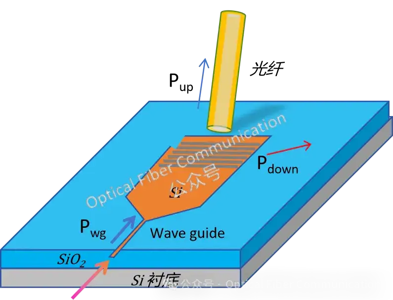
In the previous article, “Silicon Photonics Series 1: How to Smoothly Couple Light from Fiber into the Waveguide?“, we mentioned that a grating-coupling approach can be used.
Below, let us look at what a grating coupler is.
A grating coupler is an optical interface device that connects optical fiber or free space to a silicon-on-insulator (SOI) waveguide. Simply put, it is a device that couples a silicon chip and an optical fiber to each other. It uses the diffraction and reflection properties of gratings to allow a light beam of a specific mode to be coupled from one environment to another.
Fiber couplers are divided into input fiber couplers and output fiber couplers. The figure above is a schematic of output fiber coupling:
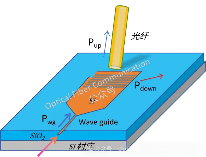
In the figure above, the fundamental TE mode is injected from the waveguide and then coupled into the fiber. When light enters the grating coupler, it is split into different propagation directions according to the grating design: part of the light diffracts upward and is received by the fiber (Pup), part diffracts downward into the substrate (Pdown), part continues to transmit forward, and part is reflected backward.
For the input fiber coupler, the opposite applies: the fundamental TE mode is injected from the fiber core and coupled into the waveguide through the grating.
To better show the internal composition of the optical coupler, let us draw a cross-section of an input fiber coupler:
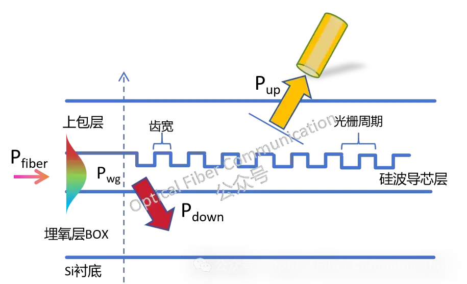
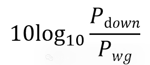
From the figure above, we can see the internal structure of this grating coupler, which is composed of several layers of different materials: the topmost layer is the upper cladding, which can be air or some oxide; then there is the silicon waveguide core layer, which is the channel for light transmission; next to it is the buried oxide layer, that is, the BOX layer, located below the silicon waveguide. Finally, below the entire structure is the silicon substrate. Among these, we use Pfiber to represent the power injected into the fiber, Pwg to represent the optical power entering the coupler, and Pup and Pdown to represent the optical power transmitted upward and entering the substrate downward, respectively. These parameters jointly determine the operating efficiency and performance of the grating coupler. Through the definition of the above parameters, we can calculate the coupling efficiency of the grating coupler, that is, the insertion loss IL:

The transmission loss can also be calculated:
Among these, the most important performance of a grating coupler is the coupling efficiency, which directly determines how much light is transferred from off-chip to on-chip. There are three main factors affecting the coupling efficiency of a fiber coupler: transmission loss, mode mismatch, and back-reflection.
- Transmission loss:
In the shallow-etch process, about 30% of the light energy is lost in the substrate. In the full-etch process, the transmission loss can exceed 50%.
- Mode mismatch:
The mode mismatch between the grating coupler and the fiber causes another 10% of energy loss.
- Back-reflection:
A well-designed shallow-etch grating coupler has very small back-reflection (such as -30 dB) and is not the main source of loss, but in the full-etch process, back-reflection can be as high as 30%.
Next time, let us discuss specifically how these factors cause the low coupling efficiency of fiber couplers.
Thank you for reading!
Related Reading
- Silicon Photonic Coupling: SSC Mode-Field Converters with Wedge and Slot Structures
- Tencent: Light-Source Collimated Output and SiPh Chip Coupling Decoupling
- Maximum Coupling Loss (MCL) and Maximum Path Loss (MPL)
Enjoy this article?
Subscribe to get new optical communication insights delivered to your inbox. Free, unsubscribe anytime.