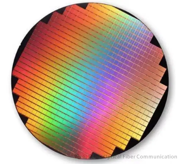
Although the final microchips are rectangular, silicon wafers are round during manufacturing. This is because the circular design offers many advantages in the production process, and round wafers are also easier to handle in subsequent processing. However, since microchips are rectangular, there are always some regions on a round wafer that cannot be fully utilized, and these regions are ultimately discarded.
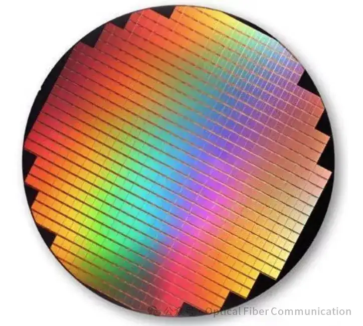
After understanding the two main silicon wafer manufacturing processes—the Czochralski process and the float-zone process—the round wafer design becomes easy to understand. Both processes produce wafers with a single-crystal structure that is naturally circular.
Although circular single-crystal silicon can be cut into rectangles, round wafers themselves offer the following advantages:
- Processing a round wafer into a rectangle introduces additional stress on its crystal structure, causing defects and dislocations that degrade wafer quality.
- Round wafers are more stable during transportation and processing, whereas rectangular wafers are easily damaged.
- In microchip manufacturing, many processes (such as chemical vapor deposition, etching, and spin coating) are radially symmetric, and round wafers are easier to process uniformly.
- Even with rectangular wafers, the very edge regions cannot be processed effectively because these areas are prone to damage during processing. In addition, wafers need to be clamped during transport, and processing all the way to the edge may cause the outer material to peel off.
- As the wafer area increases, the proportion of wasted corner regions decreases accordingly.
However, wafers are not perfectly round. On ingots below 200 mm in diameter, a flat edge is cut, called a “flat.” On ingots 200 mm and above, to reduce waste, only a small circular notch is cut, called a “notch.”
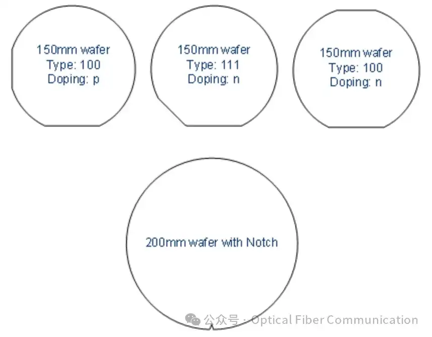
These tiny notches are used not only for wafer alignment but also cost far less in terms of wafer surface area.
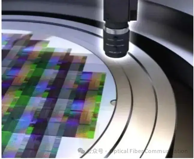
So, are all silicon wafers round? The answer is no. In solar cell manufacturing, rectangular wafers are more common. Polycrystalline silicon is typically used, and this material can be cast into a rectangular shape. Compared with microchip manufacturing, solar cell manufacturing is relatively simple, so rectangular wafers can be used, and their edges can also be chamfered.
Related Reading
- What Exactly Is the Relationship Among Wafer, Silicon Wafer, Bare Die, and Chip?
- How to Couple VCSEL Light into the PIC Wafer Plane?
- What is Strained-Layer Epitaxy?
Enjoy this article?
Subscribe to get new optical communication insights delivered to your inbox. Free, unsubscribe anytime.