Silicon wafer, silicon wafer, bare die, and chip represent the various stages of chip manufacturing. Below, let us look at the relationship among them, and by the way sort out the chip manufacturing flow.
After melting silicon raw material (sand) at high temperature and undergoing process treatment, ultra-pure polycrystalline silicon with a purity of 9-11N is obtained. Then, through the Czochralski or float-zone growth process, a cylindrical single-crystal silicon ingot is formed.
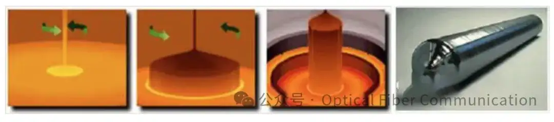
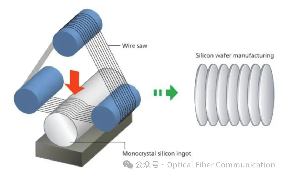
After the silicon ingot is cut with diamond wire, an original thin slice (silicon wafer/slice) is formed, whose characteristics directly determine the upper limit of the final device performance. Because the silicon ingot in the Czochralski process is cylindrical, the cut silicon wafers are naturally circular.
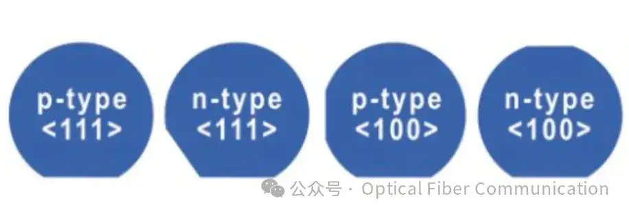
When cutting silicon ingots below 200 mm, a flat angle (Flat) needs to be machined:
Whereas silicon ingots of 200 mm and above use a circular small notch (Notch). These structures provide mechanical positioning references and crystal-orientation marks for subsequent processes.
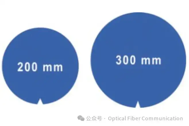
The silicon wafer size started from 2 inches (50.8 mm) in the 1960s, went through 3 inches (76.2 mm) in the 1970s, 4 inches (100 mm) in the 1980s, 6 inches (150 mm) in the 1990s, and developed to 8 inches (200 mm) and 12 inches (300 mm) in the 2000s, to meet the needs of higher integration and lower cost.
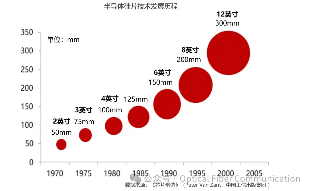
The silicon wafer needs to undergo precision processing such as edge grinding, lapping, and chemical mechanical polishing (CMP), transforming it into a silicon wafer with an atomically flat surface.
Taking a 300 mm wafer as an example, if enlarged to the diameter of the Earth (12,742 km), its surface undulation would be equivalent to hills of less than 3 m in height (actual flatness < 20 nm). At this point, the silicon wafer has transformed into a substrate platform meeting semiconductor manufacturing requirements.

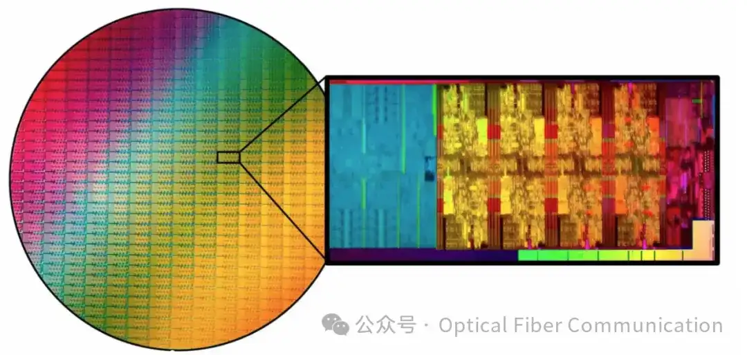
On the silicon wafer, arrayed functional units are formed through hundreds of processes such as lithography and etching. Each independent unit is called a die (bare die), containing a complete transistor circuit, interconnect structure, and I/O pads.

In the figure below, the circular one is the wafer, and the square ones in it are the dies, that is, bare dies.
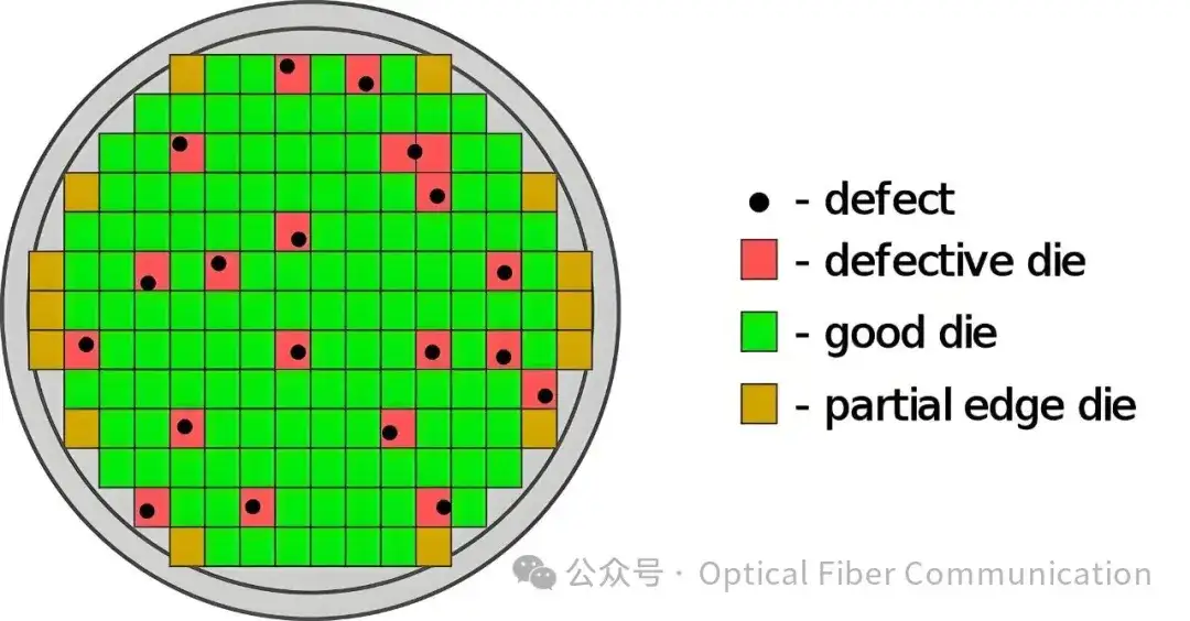
After completing all wafer-level manufacturing processes, wafer testing/probing is required, using a probe card to contact the pads on the die to screen out functionally qualified dies (usually marked as Good Die). Then, through the dicing/sawing process, the wafer is divided into individual die units along the scribe lines.
A bare die itself does not have physical protection and electrical connection capability, so it needs to go through the packaging process: mounting onto a substrate, wire bonding or flip-chip interconnection, and adding an epoxy resin or ceramic sealing shell, finally forming a directly applicable chip.

The silicon ingot is ultra-high-purity single-crystal silicon material; the silicon wafer is the original thin slice cut from the ingot; the silicon wafer is a standardized substrate after precision processing; the bare die is an unpackaged unit with circuit functionality on the wafer; and the chip is the end product after packaging and testing.
Thank you for reading!
Related Reading
- How Exactly Is a Silicon Wafer Manufactured?
- How to Couple VCSEL Light into the PIC Wafer Plane?
- Is This Wafer-Level Packaging?
Enjoy this article?
Subscribe to get new optical communication insights delivered to your inbox. Free, unsubscribe anytime.