Silicon wafers are very familiar to those of us in the semiconductor industry. But in fact, they are thin slices cut from large single-crystal silicon grown from molten electronic-grade polysilicon.
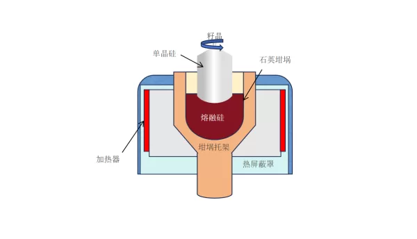
The process used to grow these single crystals is named after its inventor Jan Czochralski and is called the Czochralski process. The figure below shows the basic steps and components involved in the Czochralski process.

The Czochralski process is carried out in an evacuable chamber, usually called a “crystal puller”, which contains a large crucible (usually made of quartz) and an electric heating element.
Semiconductor-grade polysilicon is loaded (charged) into the crucible, together with precisely measured amounts of any dopants (such as phosphorus or boron) that may be needed to give the product wafer specific P-type or N-type characteristics. Evacuation removes the air in the chamber to avoid oxidation of the heated silicon during growth. The loaded crucible is heated electrically to a temperature high enough to melt the polysilicon (above 1421°C). Once the silicon is completely molten, a small seed crystal mounted on a rod is lowered and immersed in the molten silicon. The seed crystal is usually about 5 mm in diameter and up to 300mm in length. It serves as the “starting point” for growing a larger silicon crystal from the melt. The seed crystal is mounted on a rod, with its known crystal plane oriented vertically in the melt (the crystal plane is defined by “Miller indices”). For the seed crystal, crystal planes with Miller indices of <100>, <110>, or <111> are usually selected.
The crystal grown from the melt will follow this initial orientation, so that the final large single crystal has a known crystal orientation. After immersion in the melt, as the larger crystal grows, the seed crystal is slowly pulled (a few centimeters per hour) out of the melt. The pulling speed determines the diameter of the final large crystal. During crystal pulling, both the crystal and the crucible rotate to improve the uniformity of the crystal and dopant distribution. The final large crystal is cylindrical; it is called a “boule”.
The Czochralski growth method is the most economical way to produce silicon boules suitable for general semiconductor device manufacturing (called CZ silicon wafers). This method can form boules large enough to produce silicon wafers up to 450 mm in diameter. However, the method has certain limitations. Since the boule is grown in a quartz (SiO2) crucible, there is always some oxygen contamination in the silicon (typically 10^18 atoms/cm³ or 20 ppm). Graphite crucibles were once used to avoid this contamination; however, this introduces carbon impurities into the silicon, although at a concentration one order of magnitude lower. Both oxygen and carbon impurities reduce the minority carrier diffusion length in the final wafer. The axial and radial doping uniformity in Czochralski silicon is also limited, making it difficult to obtain wafers with resistivity greater than 100 ohm-cm.
Higher-purity silicon can be produced through a purification method called Float Zone (FZ) refining. In this method, a polysilicon ingot is mounted vertically in a growth chamber under vacuum or inert atmosphere. This ingot does not contact any components in the chamber except the ambient gas and a seed crystal of known orientation at its bottom, as shown in the figure below.

The silicon ingot is heated by a non-contact radio frequency (RF) coil, establishing a zone of molten material (molten zone) in the ingot, usually about 2 cm thick. In the FZ process, the silicon rod moves vertically downward so that the molten zone moves upward along the length of the ingot, pushing impurities toward the front of the molten zone and leaving highly purified single-crystal silicon behind. The resistivity of FZ silicon wafers can be as high as 10000 ohm-cm.
After the silicon boule is produced, it is cut into lengths convenient for handling, and each length is ground to the desired diameter. At this stage, orientation flats indicating the doping type and orientation of the wafer are also ground on the boule, used for wafers smaller than 200 mm in diameter. For wafers smaller than 200 mm, the primary flat (the largest) is perpendicular to the designated crystal axis, such as <111> or <100>.

The secondary flat (smaller) indicates whether the wafer is p-type or n-type. 200 mm (8-inch) and 300 mm (12-inch) wafers use a single notch oriented toward a designated crystal axis to indicate wafer orientation, with no mark for doping type.
After the boule is ground to the desired diameter and the orientation flats are formed, it is cut into thin slices using diamond-coated blades or wire saws. At this stage, the edges of the wafer are usually rounded. At the same time, laser marking is added near the primary flat, indicating wafer type, resistivity, manufacturer, and other information. The unprocessed wafer is ground and lapped/polished on both sides to bring all wafers to the specified thickness and flatness tolerances. Grinding brings the wafer to rough thickness and flatness tolerances, and the subsequent lapping/polishing process removes the last bit of unwanted material from the wafer surface, leaving a smooth, flat, unpolished surface. Lapping/polishing can usually achieve a wafer surface flatness uniformity tolerance of less than 2.5 um.

The final stages of wafer manufacturing include: first, chemical etching to remove any surface layer that may have accumulated crystal damage and contaminants during cutting, grinding, and lapping/polishing; followed by chemical mechanical polishing (CMP), which produces a highly reflective, scratch-free, and damage-free surface on one side of the wafer. Chemical etching is done with an etchant composed of hydrofluoric acid (HF) mixed with nitric acid and acetic acid, which dissolves silicon. In CMP, wafers are mounted on carriers and placed into a CMP machine, where they undergo a combination of chemical and mechanical polishing to reduce surface roughness to about 1 nm (or down to 0.5 nm where feasible).

Usually, CMP uses a hard polyurethane polishing pad with a slurry composed of finely dispersed alumina or silica abrasive particles in an alkaline solution. The final product of the CMP process is the silicon wafer we are familiar with as users. One side of it has a highly reflective, scratch-free, and damage-free surface on which semiconductor devices can be fabricated.
Wafer specifications should include diameter, crystal orientation, surface polish type, doping type, and resistivity. The thickness of the wafer depends on its diameter; manufacturing convention limits the thickness to a maximum of about 2 mm, while fracture risk limits the minimum thickness to 200 um. The thickness tolerance is independent of wafer diameter, specified as +/- 25 um; measured values are usually lower (+/- 15 um).
The degree to which the wafer deviates from an ideal cylindrical shape is characterized by the following parameters:
- TTV: Total Thickness Variation (the difference between the minimum and maximum thickness of the wafer);
- Bow: the maximum deviation of the median plane relative to a reference plane (bow);
- Warp: the deviation of the wafer’s median plane relative to a reference plane corrected for bow (warp).
For wafers 4 inches in diameter and below, the TTV specification requires less than 10 um; larger-diameter wafers allow higher TTV values. For wafers up to 4 inches, the bow specification requires less than 40 um; larger-diameter wafers allow larger bow limits. For wafers up to 4 inches, the warp specification requires less than 50 um, and larger-diameter wafers allow higher warp values.
Related Reading
- What Exactly Is the Relationship Among Wafer, Silicon Wafer, Bare Die, and Chip?
- How to Couple VCSEL Light into the Plane of a PIC Wafer?
- Is This Wafer-Level Packaging?
Enjoy this article?
Subscribe to get new optical communication insights delivered to your inbox. Free, unsubscribe anytime.