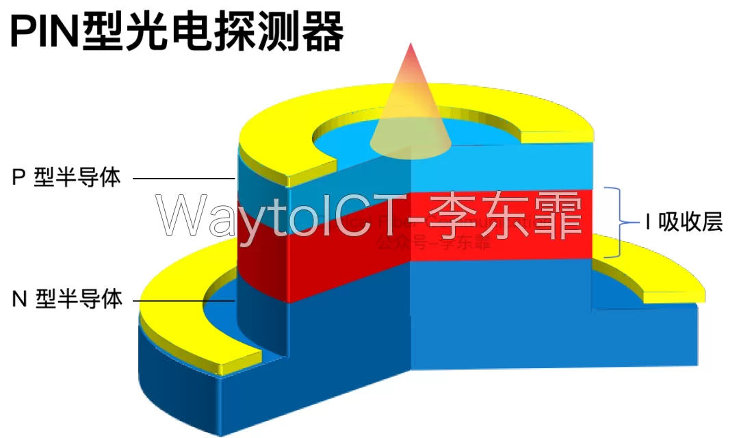
A conventional Si-PIN photodiode adds an I layer, also called the intrinsic layer, between the P-type and N-type semiconductors, usually used as the absorption layer.
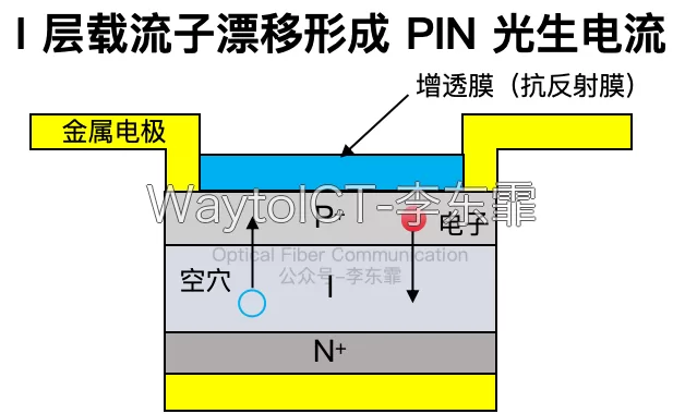
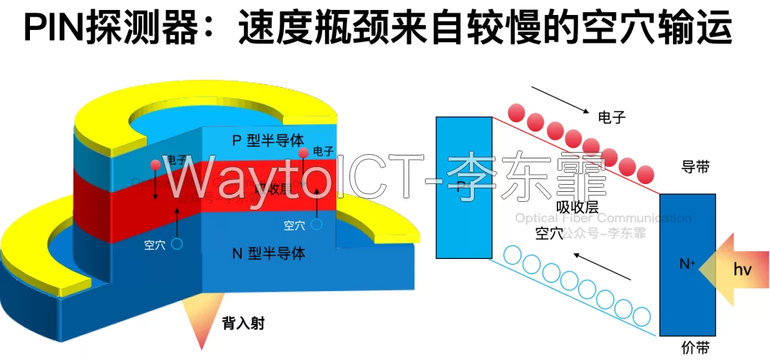
After absorbing photons, the I layer generates electron-hole pairs. Under the reverse bias electric field, electrons drift toward the N side and holes drift toward the P side, and the two types of carriers together form a photocurrent.
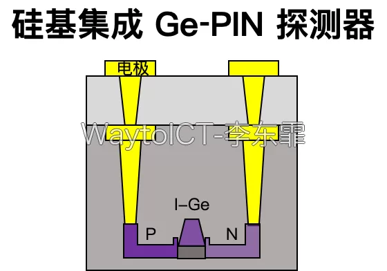
The absorption layer does not necessarily use silicon. For example, InP-based InGaAs PIN uses InGaAs as the absorption layer, and silicon-based integrated Ge-PIN detectors use a Ge thin film as the absorption layer.
Related reading: IMEC’s Evolution of Germanium-Silicon PD and APD Detector Technology | University of Tokyo: Technical Progress in Photonic Computing and Multi-Port Ge Detectors | Marvell: Two New Schemes to Improve the Bandwidth of Silicon-Germanium Detectors | Huawei: C+L Band 100G Bandwidth Germanium-Silicon Photodetector with Stress Layer
Ideally, the I layer is completely intrinsic and undoped; in practice, whether intentionally or not, it has some low-concentration weak doping.
In a conventional PIN, both electrons and holes contribute to the photocurrent, and their speed of moving to the two sides in the depletion layer affects the photoresponse speed, that is, the bandwidth.
Since the electron drift velocity is much faster than that of holes, the carrier transit time limitation comes mainly from holes.
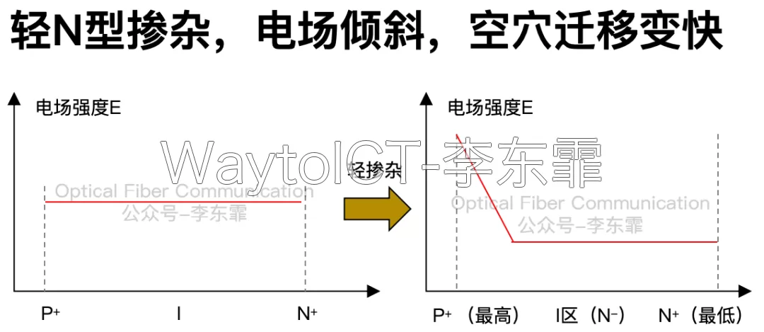
Therefore, to make holes drift faster, light N-type background doping can be used.
In this way, the electric field in the depletion region is no longer flat and uniform, but gradually increases from the N side to the P side. As holes drift toward P⁺, they pass through a stronger electric field, so the drift velocity is faster.
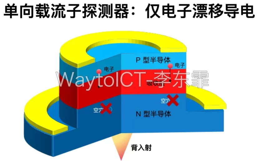
But in this scheme, holes are still the main bandwidth limitation and cannot be completely eliminated. Another more thorough approach is to collect only electrons, making electrons the main carriers, while holes do not participate in conduction.
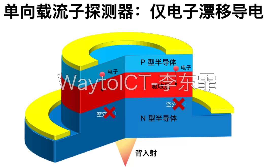
Specifically, under an applied voltage, the electron collection layer generates a strong electric field, and photogenerated electrons move from the absorption layer to the collection layer. The photocurrent is basically entirely generated by the electrons from the absorption layer.
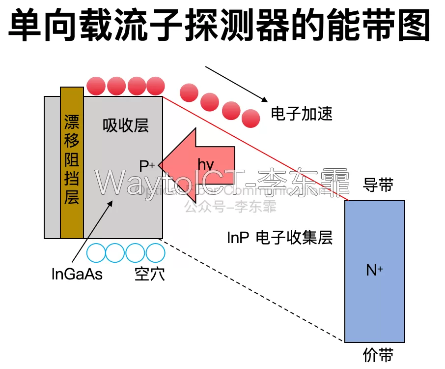
The drift blocking layer mainly blocks holes from entering the drift region, while electrons enter the drift layer and are ultimately collected by the collection layer.
This kind of detector in which only electrons participate in the photocurrent is called a uni-traveling-carrier photodetector, abbreviated UTC-PD.
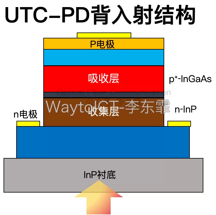
Unlike a conventional PIN, the UTC-PD separates the absorption region from the drift collection region: the absorption region is heavily doped p⁺-InGaAs, and the drift collection region is n-InP.
Holes do not need to travel a long drift path, and the limitation of slow holes on bandwidth is eliminated, so very high bandwidth can be achieved.
However, shortening the carrier transit path can improve bandwidth but also reduces optical absorption. The light can be made to enter the detector in an edge-coupling manner through refraction, that is, a waveguide UTC-PD.
Related reading: Fundamentals: Waveguide Photodetectors
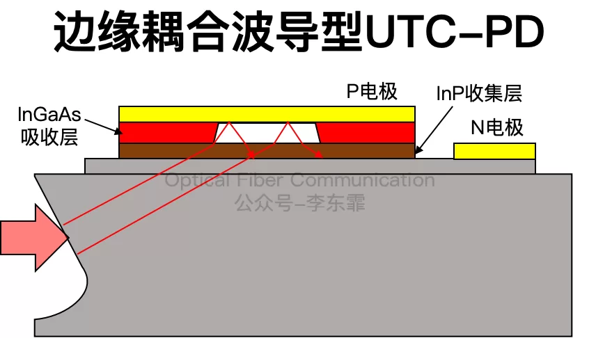
Light is incident on the inclined surface and refracted, then obliquely incident on the absorption layer at a certain angle. Compared with direct back illumination, this increases the optical absorption area.
Thanks for reading.
Please forgive any inaccuracies!
The compilation report on Optical Chips, Optical Devices, and Optical Transceivers (OFC2026), printed in color and bound in A4, consists of two volumes totaling 525 pages, about 200,000 characters. If you need it, welcome to contact us to order, at a favorable price!
WeChat contact: WaytoICT
Further Reading
- Fundamentals: Waveguide Photodetectors
- Huawei: C+L Band 100G Bandwidth Germanium-Silicon Photodetector with Stress Layer
- Fundamentals: Photoelectric Effect and Electro-Optic Effect
- Fundamentals: Eye Diagram
Enjoy this article?
Subscribe to get new optical communication insights delivered to your inbox. Free, unsubscribe anytime.