Compared with the Mach-Zehnder modulator (MZM), the microring modulator (MRM) is smaller in size and offers higher bandwidth density. The MRM is well suited for high-density integration scenarios such as co-packaged optics (CPO).
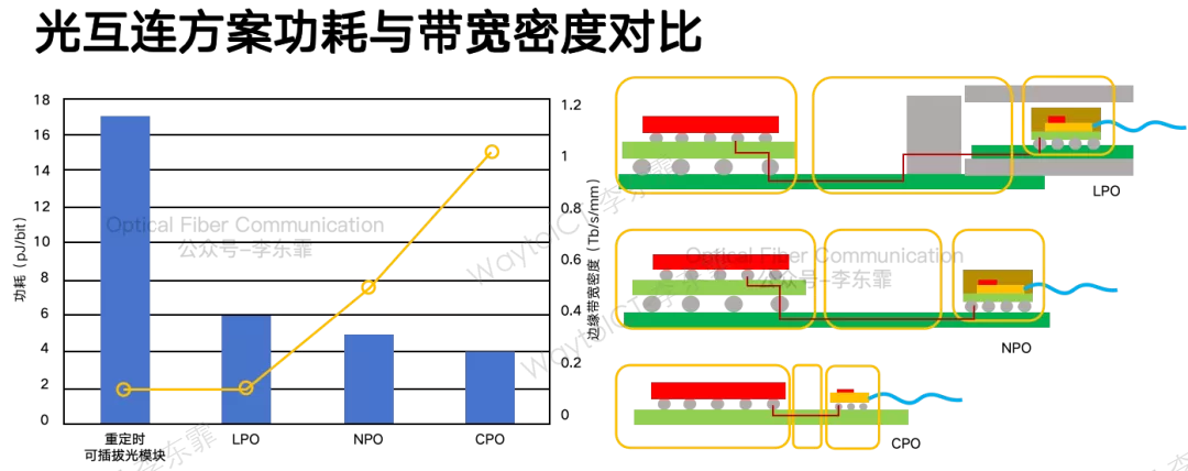
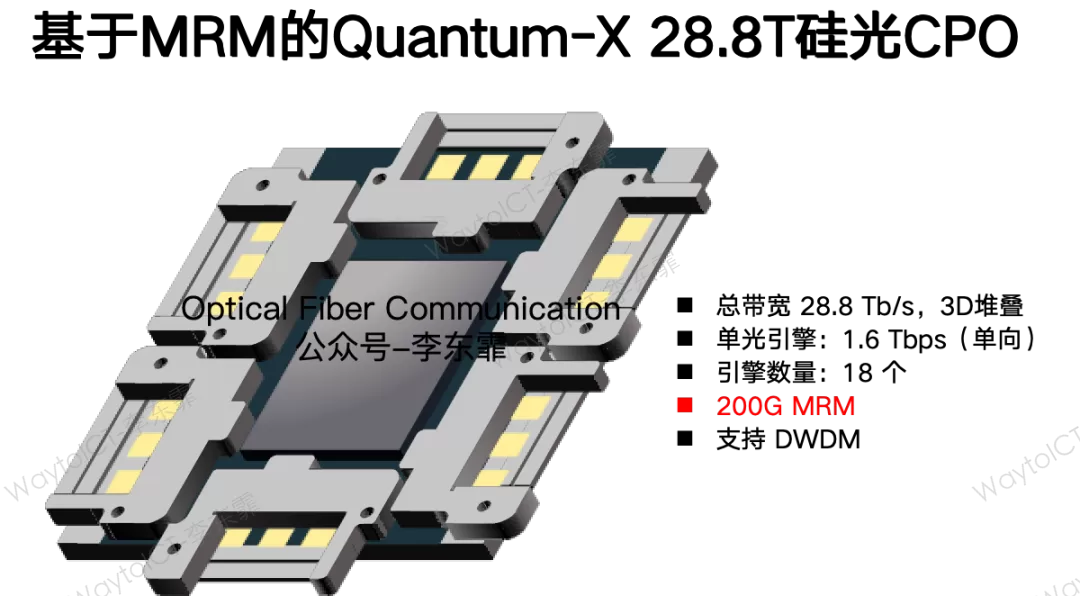
Nvidia released the world’s first CPO switch with 200Gbps per lane and 1.6Tbps total bandwidth; its microring modulator is fabricated on TSMC’s compact universal photonic engine (COUPE) process.
Recommended reading:
Nvidia: low-sensitivity microring resonators for reduced process variation
Nvidia: interconnect architecture and technical analysis of integrated silicon-photonics CPO
Lightmatter: 16-wavelength 800G BiDi microring silicon-photonics CPO solution
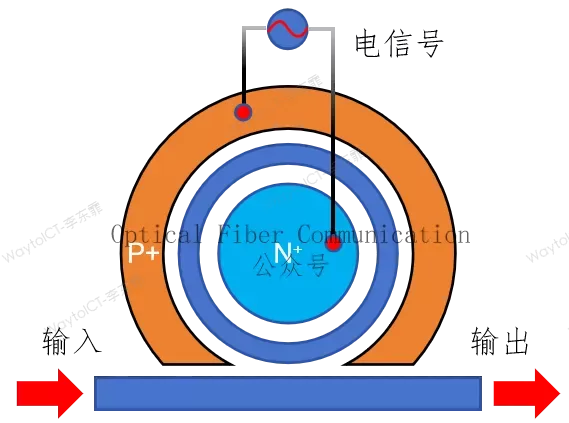
The working principle of the MRM, simply put, uses the plasma dispersion effect in silicon to modulate the effective refractive index of the waveguide via the PN-junction voltage, and then leverages the optical field enhancement of the resonant cavity to achieve efficient electro-optic modulation.
Recommended reading:
HiSilicon / Intel: SiN-SOI microring modulators for CPO
Microring resonators: coupling, modulation and wavelength-division multiplexing
For an intensity-modulated MRM, metrics such as the electro-optic bandwidth (EO BW), insertion loss (IL), linearity, modulation extinction ratio, and chirp all matter. To achieve stable transmission above 200Gbps per lane, photonics and electronics must be co-optimized.
At this year’s OFC2026, Nvidia focused on how microring modulators above 200Gbps per lane should be designed and optimized.
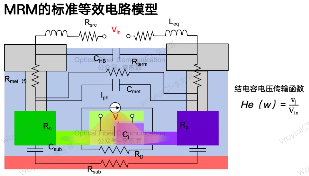
Electrically, the effective modulation voltage at different frequencies is determined jointly by the PN-junction resistance Rj, junction capacitance Cj, equivalent inductance, and the signal source and termination impedances.
These parameters constrain one another; our goal is to optimize the junction-capacitance voltage transfer function through them:
He(ω) = Vj/Vin
The PN junction of a silicon photonics modulator can be modeled as a resistance Rj in series with a junction capacitance Cj, forming a standard RC low-pass circuit.
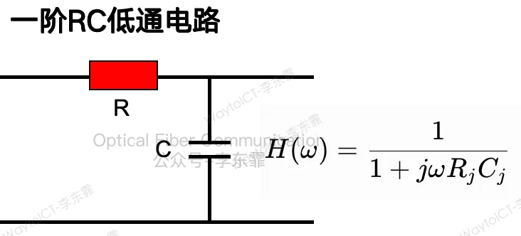
The transfer function has only one pole, and the frequency response has only one roll-off knee. Without any compensating inductance, the modulator bandwidth is inherently limited and high-frequency electro-optic signals attenuate severely.
If a small inductance Leq is added in series or parallel in the RC loop, the circuit becomes a two-pole system. The capacitance and inductance store energy with opposite phases; at low frequencies the inductive reactance is very low and the circuit still behaves mainly as an RC circuit.
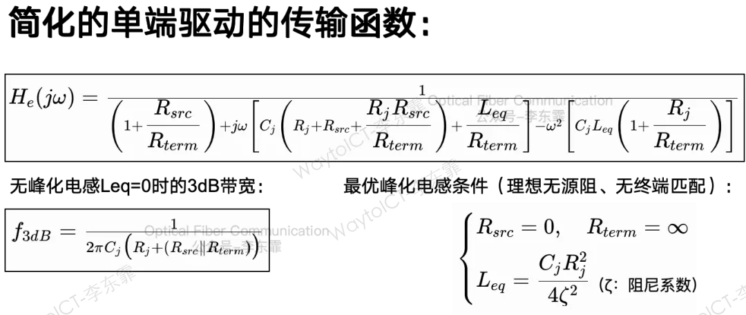
But as the frequency rises, the inductive reactance gradually cancels the signal loss caused by the capacitive reactance, creating a resonant gain bump in a specific band — that is, electrical inductive peaking, which effectively compensates high-frequency attenuation.
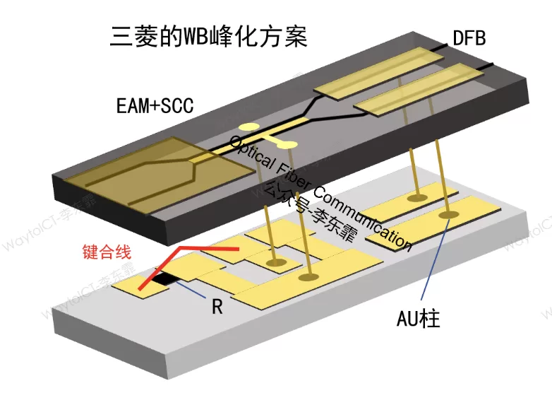
As we discussed earlier, an EML can introduce peaking inductance through wire bonding to raise its bandwidth.
Recommended reading:
Mitsubishi: series dual-modulator differential EML solution
Mitsubishi: from high-mesa structure to hybrid glass substrate and FC+WB high-speed EML
The optimal peaking inductance is very small, at the picohenry (pH) level. Extra parasitic R/L/C introduced by traces, bumps, and substrate will directly cancel the peaking gain or even degrade the bandwidth.
In traditional 2D or flip-chip packages, the long traces and many microbumps between the EIC driver chip and the PIC microring introduce a large amount of extra series inductance and parallel capacitance.
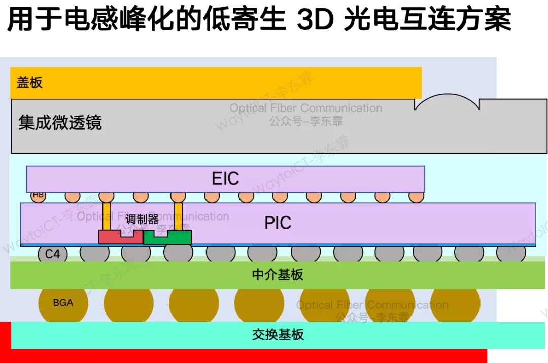
Hybrid-bonding 3D opto-electronic integration processes such as TSMC COUPE and SoIC can greatly shorten the interconnect path between the EIC and PIC, reducing the interconnect RLC parasitics.
Recommended reading:
TSMC: silicon photonics device performance and process platform for CPO
TSMC: CPO evolution roadmap based on COUPE and CoWoS packaging
3D stacking can bring the EIC and PIC physically extremely close, making the trace inductance essentially negligible.
This is a means of compensating high-frequency loss at the circuit-drive level. Note, however, that inductive peaking can only compensate the bandwidth attenuation introduced by the electrical loop.
The MRM is fundamentally a resonant-cavity device, and photons keep oscillating inside the microring. The longer photons dwell in the ring, the more pronounced the tailing of old light becomes, failing to keep up with the rapid switching of the high-speed electrical signal, causing severe attenuation of the high-frequency modulation signal and narrowing the modulation bandwidth.
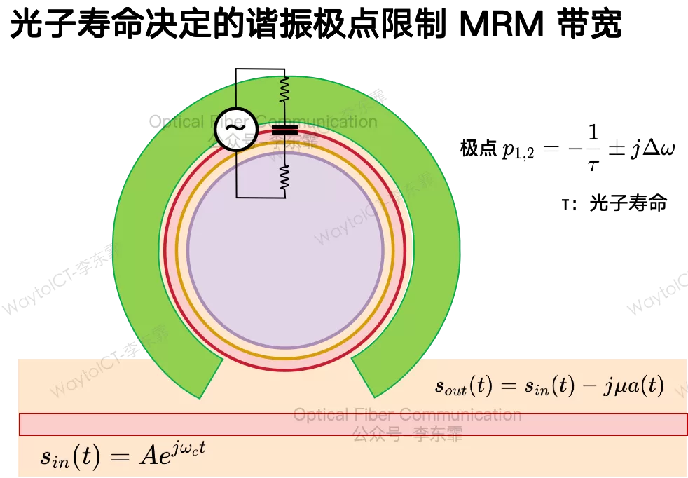
The process of residual photons slowing down the signal can be described with a pole. As long as the optical cavity has loss and photons have a dwell time, there will always be a pole.
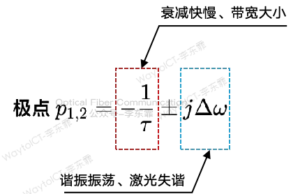
The real part of the pole is determined by the photon lifetime τ, which causes severe high-frequency attenuation: the higher the modulation frequency, the lower the output modulation gain, and the system modulation bandwidth is greatly compressed. This is an inherent defect of the resonant cavity itself and cannot be eliminated.
The imaginary part of the pole, Δω, represents how far the laser wavelength is offset from the microring resonance peak — that is, the detuning.
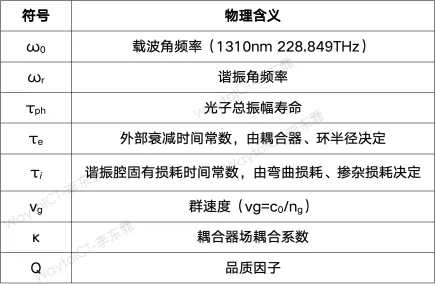
The dual-beam interference output structure of the microring, after Fourier-transforming the time-domain equations, produces a set of characteristic roots in the numerator of the transfer function — the system zeros.
These zeros can be used to cancel the pole loss described above and widen the modulation bandwidth.
The zeros are determined jointly by coupling loss, intrinsic cavity loss, and detuning. By adjusting the operating detuning, the frequency position of the zero can be shifted, using the gain lift of the zero to compensate the pole attenuation — this achieves optical peaking.
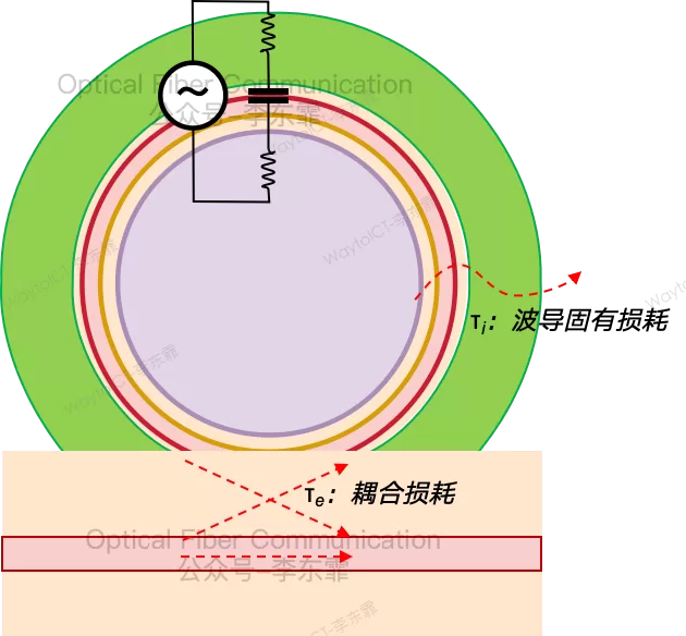
Both the photon lifetime and the position of the zero are directly related to the coupling strength of the microring, as we discussed before.
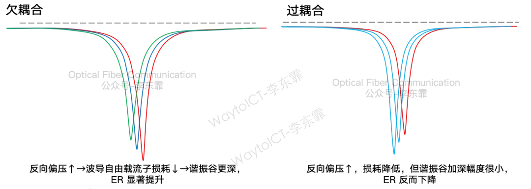
The bandwidth is determined by the detuning. However, although the optical peaking from large detuning can significantly improve the MRM high-frequency response, the cost is degraded extinction ratio and worsened nonlinearity.
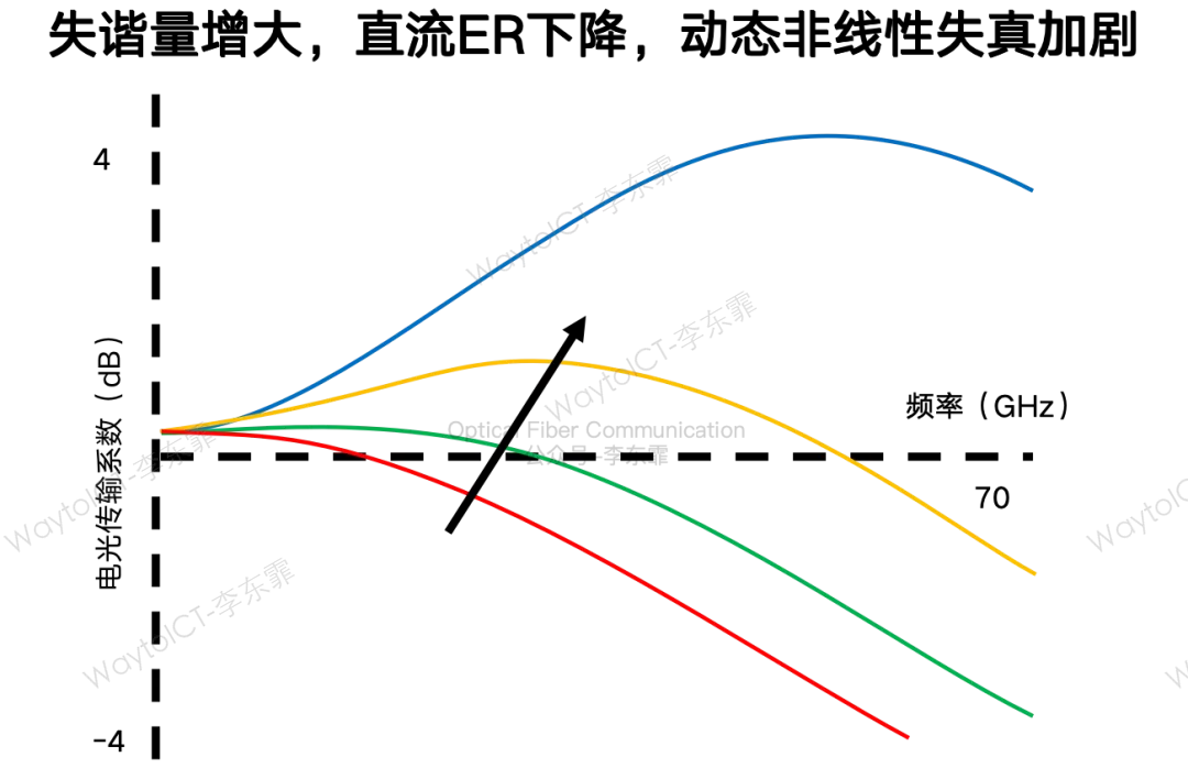
Nvidia has given a practical engineering solution — maximizing the gain-bandwidth product, with the corresponding optimal detuning Δω ≈ 1.13/τph, where overcoupled microrings generally achieve a higher gain-bandwidth product.
Currently, there is still no unified standard for benchmarking different MRMs in terms of bias conditions, performance metric definitions, and RF de-embedding procedures.
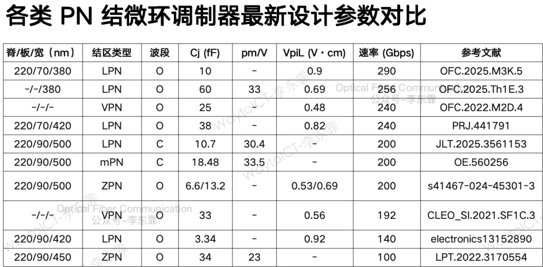
The following summarizes ultra-high-speed microring modulator results published in recent years.
Thanks for reading! Please point out any inaccuracies. Subscribe now to join our Shannon Academic ima knowledge base for free, with trustworthy Q&A based on a vast collection of papers and documents (paid-column subscribers / Knowledge Planet members only).

Thanks for your support!
Enjoy this article?
Subscribe to get new optical communication insights delivered to your inbox. Free, unsubscribe anytime.