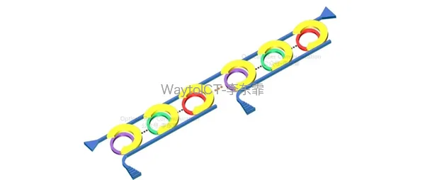
I have already written about many companies’ solutions regarding microrings, and today let me discuss it again.
- HiSilicon / Intel: SiN-SOI Microring Modulator for CPO
- Intel: A 16-wavelength 800G DWDM optical interconnect solution based on microrings
- NVIDIA: A low-sensitivity microring resonator for reducing process error
- HG Genuine: A CPO silicon photonic engine with cascaded Bragg gratings and microrings
Starting from the FP Cavity
Let me start with the FP cavity. Its principle is that light travels back and forth between two parallel reflecting surfaces. When twice the distance between the two mirrors (the optical path difference) is an integer multiple of the wavelength, constructive interference occurs, forming a transmission peak.
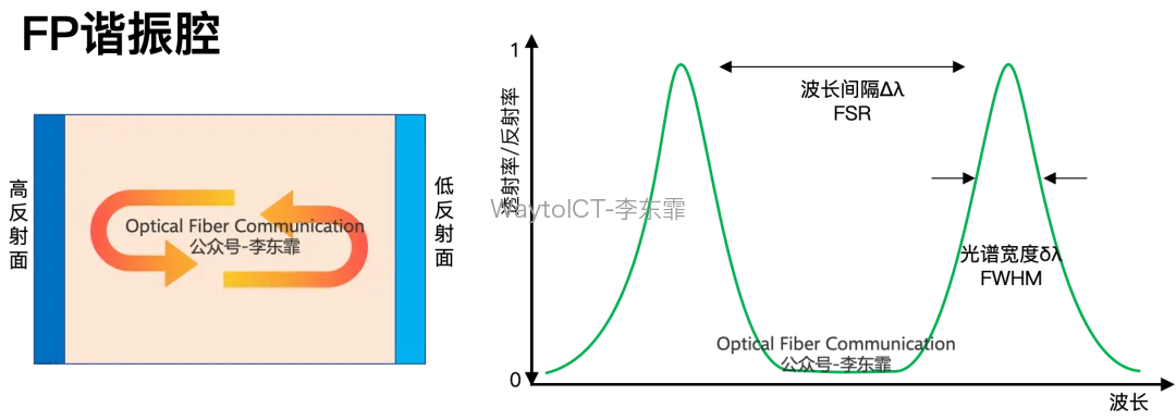
When the optical path difference is an odd multiple of half the wavelength, destructive interference occurs, and the light is reflected and cannot transmit.
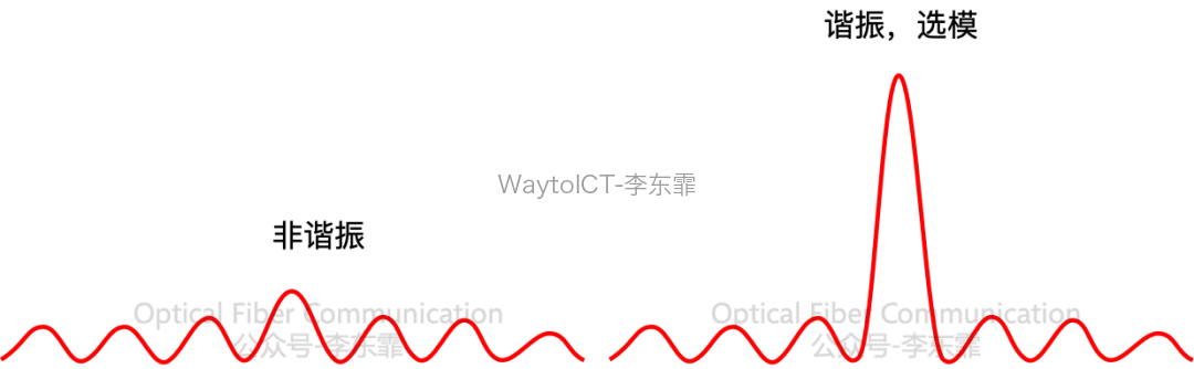
In general, in a waveguide with an interference structure, wavelengths satisfying the resonance condition undergo multi-beam constructive interference, manifesting as field enhancement and high transmission; non-resonant wavelengths are reflected or suppressed by destructive interference.
Grating: Cascaded FP Cavities
A similar structure is the grating. It can be regarded as a cascade of multiple FP cavities, using multi-level constructive interference produced by periodic refractive-index variation to provide mode selection and high reflection in specific bands.
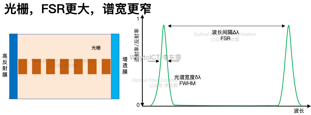
Compared with the FP cavity, the grating has a wider FSR and a narrower spectral width. Therefore, lasers composed of FP cavities are usually multimode, while DFB lasers composed of gratings can achieve single-mode output.
From Standing Wave to Traveling Wave: Why Make It a Ring
Both the FP cavity and the grating let light reflect back and forth between two points, forming a standing wave. When L = mλ is satisfied, multi-beam constructive interference occurs to achieve frequency selection.
But this has structural limitations: the optical path can only be accumulated by increasing the device length, resulting in a large device size; and when light reflects back, it is very susceptible to reflection interference.
If the waveguide is made into a ring so that it becomes a resonant cavity, light no longer needs two mirrors to reflect back and forth; instead, it travels in a single direction to form a traveling wave, so the size can be made very small and reflection interference is almost eliminated.
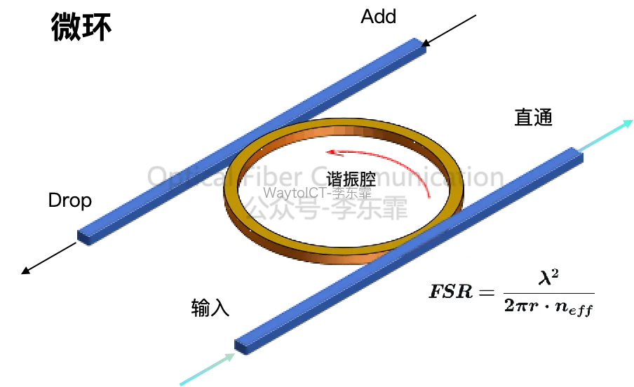
Structural Choice of Microring Modulators
When a microring is used for an optical switch, the straight-waveguide bus can be placed parallel or crossed; when used for a modulator, a ring or racetrack shape is usually adopted, and waveguide crossings are strongly avoided.
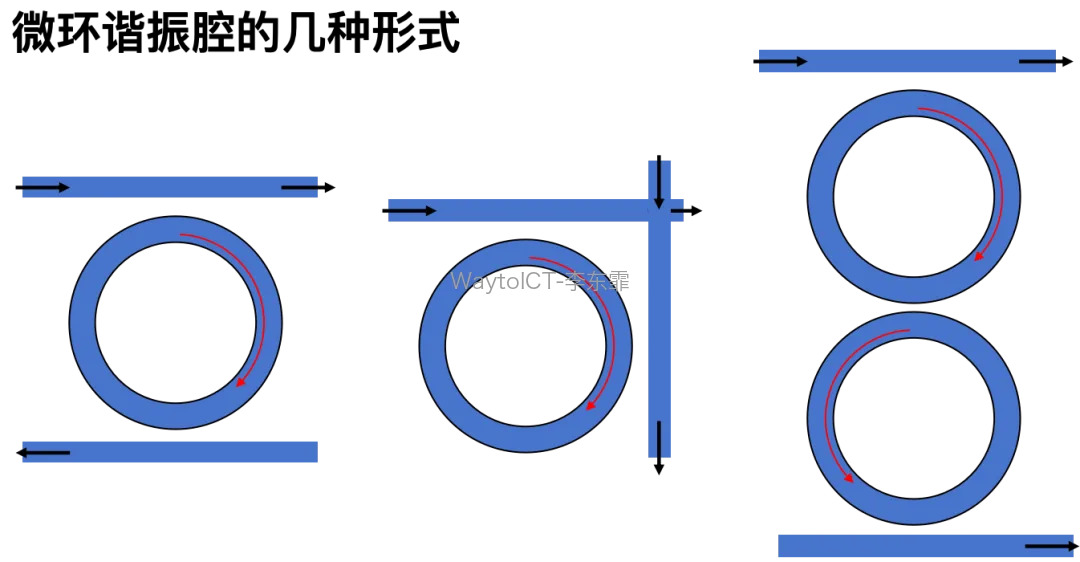
What we commonly see in theory is a pure circular ring with no straight segment (Lc = 0), where coupling occurs only at one point. But it is rarely seen in large-scale manufacturing, mainly because this point-coupling efficiency is extremely low.
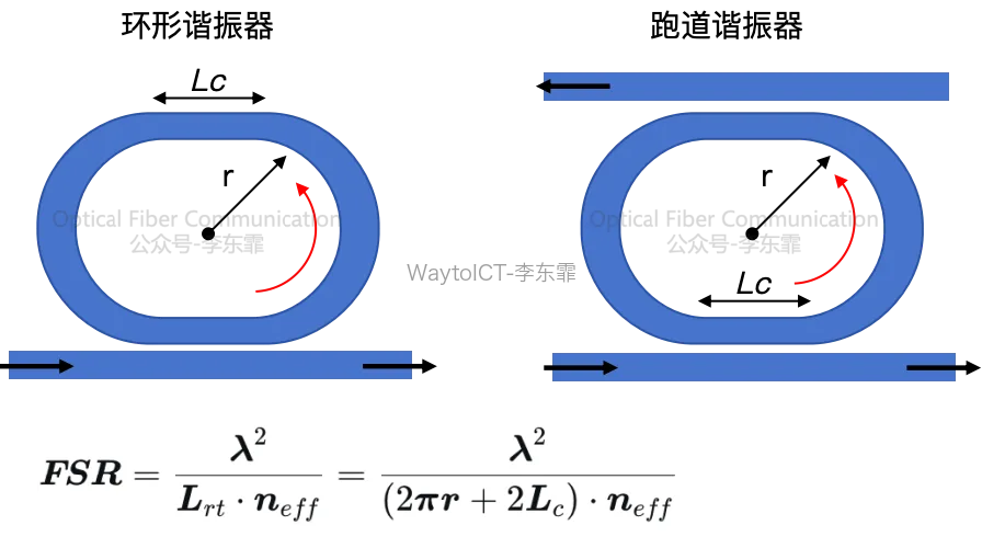
Especially when we want to use a microring as an electro-optic modulator, changing the refractive index by applying voltage requires doping on the waveguide (such as a PN junction) or attaching heating electrodes, which makes the straight waveguide segment even more necessary.
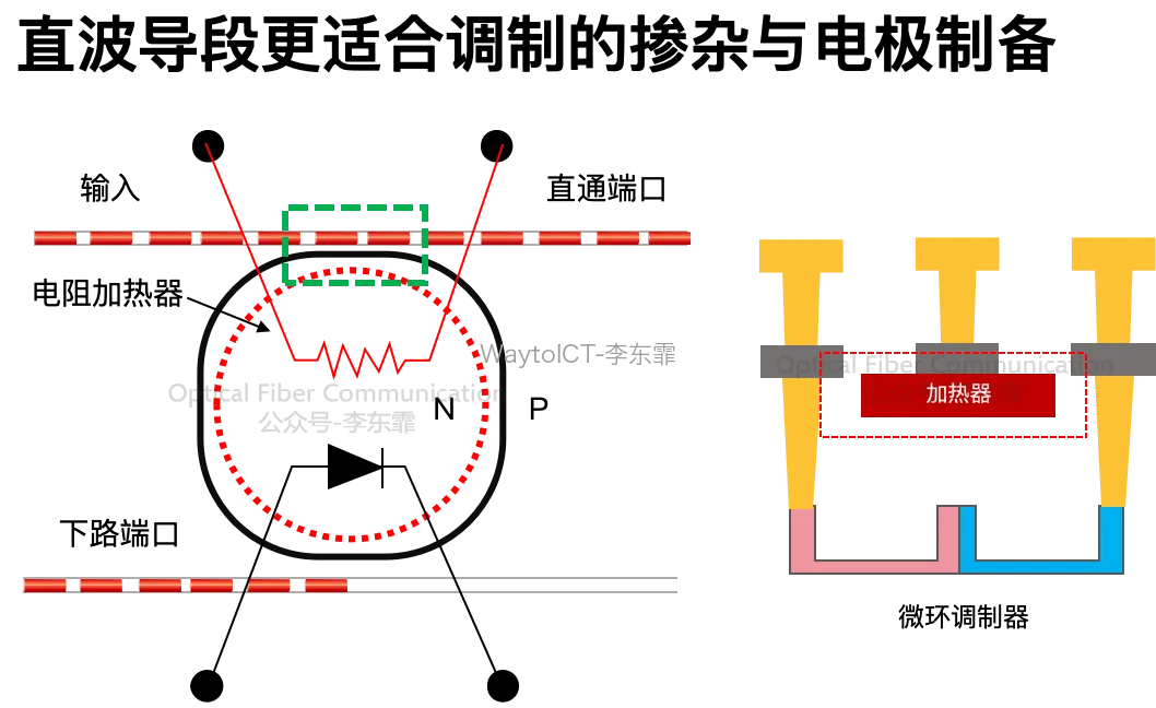
Uniform doping and electrode attachment on a bent waveguide are very difficult and prone to extra loss; whereas operating on a straight segment greatly reduces process difficulty and achieves higher modulation efficiency.
Trade-off Between FSR and Q Factor
Compared with gratings, the FSR of microrings is much larger. The smaller the microring radius, the larger the FSR, the wider the usable resonance-wavelength window, the more channels that can fit within a single FSR, and the less likely other resonance peaks will cause crosstalk.
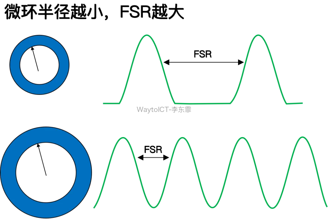
A small radius also reduces chip area, benefiting high-density silicon photonic integration. But too small a radius causes bending loss to rise sharply (Q factor plummets), and process tolerance deteriorates.
However, when a microring is used as a modulator, the loaded Q factor must be reduced in exchange for modulation bandwidth; otherwise, an overly long photon lifetime will limit the bandwidth. Therefore, its actual linewidth is wider than that of a grating that maintains a high Q factor.
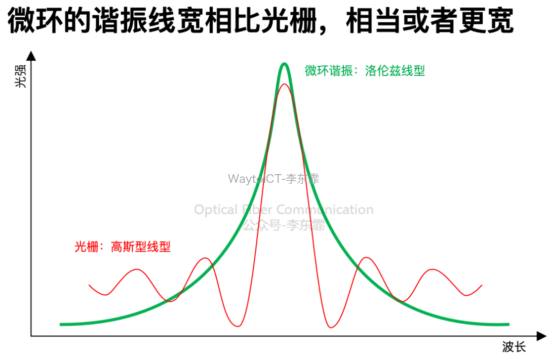
Specifically, the higher the Q factor, the more rounds photons travel inside the microring and the longer the dwell time (photon lifetime), which manifests on the spectrum as a narrower resonance-peak linewidth (δλ).
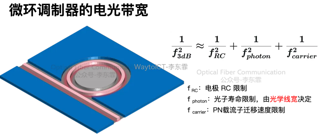
The actual electro-optic bandwidth of a microring modulator is jointly determined by three factors, roughly satisfying the following formula:
How Modulation Is Achieved
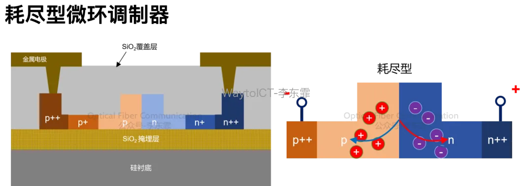
Specific modulation is achieved as follows: applying a voltage produces an electro-optic (or thermo-optic) effect, changing the effective refractive index of the microring waveguide, causing the resonance wavelength to shift, and ultimately causing the output optical power to change.
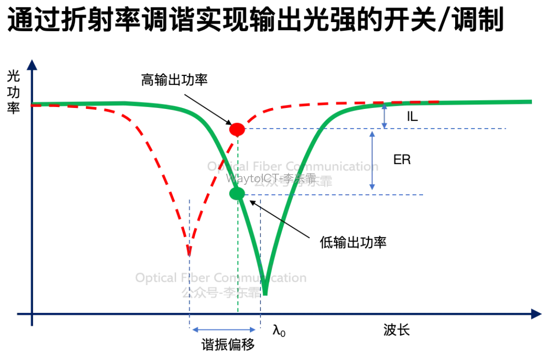
Currently, silicon-based microring modulators are the most mature. Carrier-injection, accumulation, and depletion types are all applicable in principle, but microring modulators mainly adopt the depletion type; the accumulation type is rare, and the injection type is limited by speed.
Microring Optical Switches
We also mentioned microring optical switches above; let me briefly describe them here. Their principle is similar to that of modulators: applying voltage changes the refractive index to shift the resonance wavelength, controlling the on-off switching of light at a specific wavelength between the through port and the drop port.
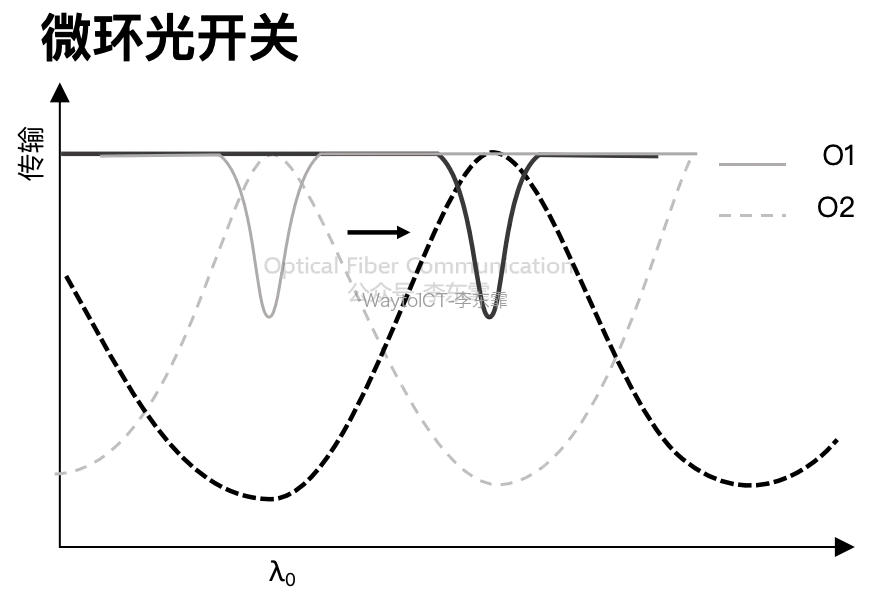
Multiple microring resonant cavities can be cascaded in series to form a cascaded microring optical switch, and the Vernier effect can extend the FSR to support more wavelength channels.
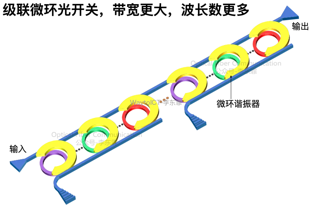
Compared with a single microring switch, the cascaded structure has an extremely high out-of-band rejection ratio, can greatly suppress out-of-band optical signals, and has lower crosstalk.
Thank you for reading.
Please forgive any inaccuracies!
Related Reading
- NVIDIA: Design Approach for a High-Speed Microring Modulator Beyond 200G per Lane
- HiSilicon / Intel: SiN-SOI Microring Modulator for CPO
- Microring Resonators: Coupling, Modulation, and Wavelength-Division Multiplexing
Enjoy this article?
Subscribe to get new optical communication insights delivered to your inbox. Free, unsubscribe anytime.