In co-packaged optics (CPO), the electrical integrated circuit (EIC) and photonic integrated circuit (PIC) are typically integrated through 3D stacking, which brings clear benefits: shorter interconnect distances, higher bandwidth density, and lower power consumption.
Two main approaches are used today: one is through-silicon vias (TSV) drilled directly through the chip, and the other is high copper pillars in a fan-out package.
Let us look at the first approach, where the PIC is placed on top of the EIC.
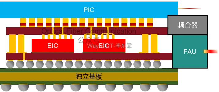
In practice, however, fabricating through-silicon vias in an electrical chip is relatively complex, so wafer-level fan-out processes are more commonly used today to form tall copper pillars that connect to the photonic chip. This structure also makes it easier to let the photonic chip extend slightly outward to support edge optical coupling.
The other approach reverses the order, placing the PIC on the bottom. In this case, the through-silicon vias on the photonic chip can be used to connect to the electrical chip above.
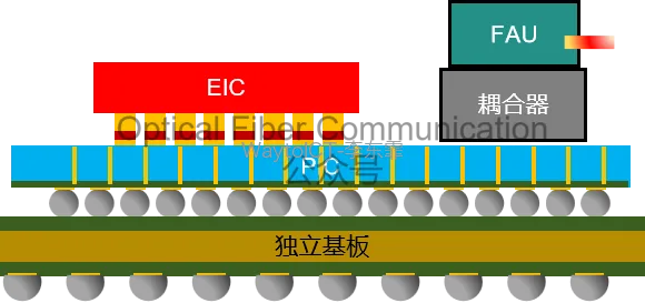
This layout has two points that require special attention: how the fixed assembly unit is installed, and how to control the warpage of the photonic chip.
The advantages are better thermal dissipation and electrical performance, supporting data rates of 200G/lane and above.
Now let us turn to how optical fiber connects to the photonic chip. There are several technology choices here: active alignment versus passive alignment, and edge coupling versus grating coupling.
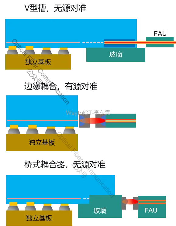
For more on edge and vertical coupling schemes and examples, see:
An innovative CPO fiber vertical coupling scheme Vertical and edge coupling: MEMS-based cantilever edge couplers
If better optical performance is desired — lower loss and less wavelength sensitivity — lensed active edge coupling generally delivers better results.
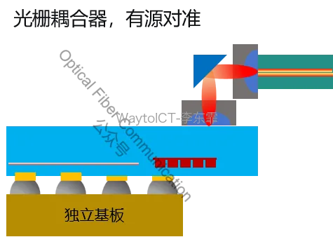
For large-scale production, however, wafer-level solutions are more practical, such as passively aligned on-wafer mirror couplers.
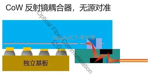
The industry currently adopts wafer-level assembly widely. In mass production of CPO devices, vertical couplers are typically used to complete optical assembly and fixed-unit integration.
These couplers can expand the spot size, thereby relaxing alignment tolerance, and support wafer-level testing and detachable design while being wavelength-insensitive, which also makes them suitable for dense wavelength-division multiplexing (DWDM) systems.
Recommended reading:
Samtec: CPX supporting CPC + CPO
1.6T DR8 optical engine and coupling methods
Nvidia: CPO external laser coupling with polarization tracker
If you are interested in semiconductors, optical devices, optical modules, and fiber-optic communications, welcome to follow us!
Enjoy this article?
Subscribe to get new optical communication insights delivered to your inbox. Free, unsubscribe anytime.