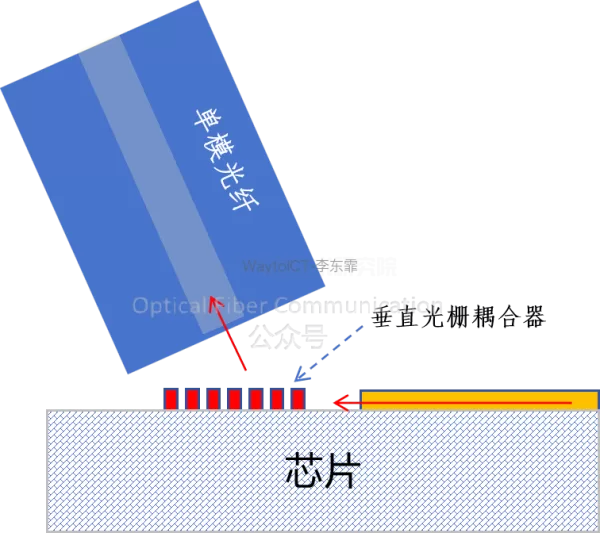
This is a WaytoICT paid-reading column. The full technical analysis and accompanying schematics require a ¥9.9 payment to unlock! To solve the above problems, optical fiber vertical coupling technology was developed. Because it can efficiently connect the fiber and chip, especially saving lateral space, it has become the primary coupling method in silicon photonics. Currently…
SMIC’s Innovative Silicon-Germanium Planarization Process
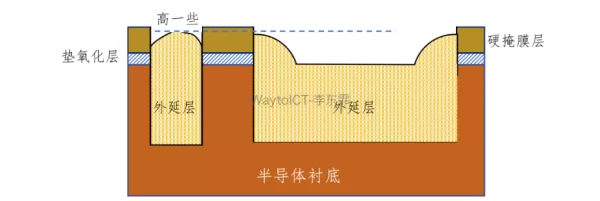
This is a WaytoICT paid-reading column. The full technical analysis and accompanying schematics require a ¥9.9 payment to unlock! During epitaxial growth, the sidewall positions of a wide trench are squeezed by the sidewall and generally bulge somewhat, making this small portion protrude above the height of the main body of the epitaxial layer. Of…
Understanding the Semiconductor-Grade Silicon Process Flow in One Article
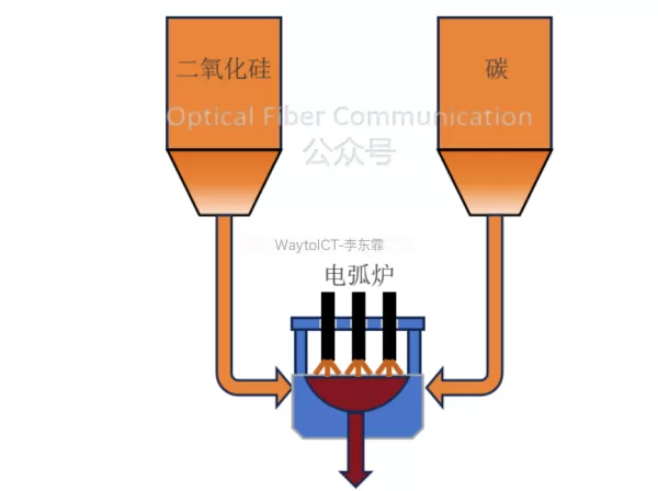
This is a WaytoICT paid-reading column. The full technical analysis and accompanying schematics require a ¥9.9 payment to unlock! Silicon (Si), as the second most abundant element in the Earth’s crust, naturally exists in silicate rocks and sand. The elemental silicon used to manufacture semiconductor devices has its raw material in high-purity quartz and quartz…
Limitations of Conventional IM-DD Systems
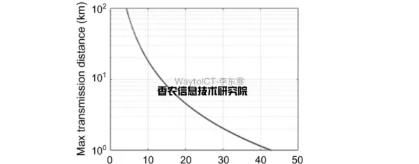
This article is part of the WaytoICT paid reading column. The technical analysis and accompanying schematics require a ¥9.9 payment to unlock! The figure below shows the functional relationship between L_max and f_BW. It can be seen that the maximum achievable distance of IM-DD systems declines sharply as the symbol rate increases. For example, over…