Although the growth of lattice-matched layers is very important for manufacturing reliable semiconductor lasers, we can also use materials with a small degree of lattice mismatch to manufacture high-quality semiconductor lasers. This lattice mismatch produces strain in the epitaxial layer, thereby changing the band structure of the semiconductor. The typical value of the tolerable strain Δa/a for lattice mismatch is less than 1.5% (where a is the lattice constant of the substrate, and Δa is the lattice constant difference between the substrate and the epitaxial layer). The greater the strain, the thinner the dislocation-free layer that can be grown on the substrate. Beyond a certain thickness (the critical thickness), a large number of dislocations are produced, and the luminescence properties of the material become very poor. Below are two material systems that have been widely studied for manufacturing strained-layer lasers:
- InGaAsP active region grown on InP;
- InGaAs active region grown on GaAs.
The emission wavelength range of the former is 1.2-1.6 μm, and that of the latter is 0.85-1.05 μm. Both types of strained-layer lasers have some advantages, which we will leave for later articles. In addition, the InGaAsP semiconductor alloy can also be lattice-match-grown on InP. Non-lattice-matched layers are mainly grown by MOVPE and CBE growth techniques. The composition of the layer can be changed by varying the flow rate of one of the substances.
The In concentration in the In1−xGaxAs epitaxial layer grown on InP as a function of the TMIn flow rate is shown in the figure below.
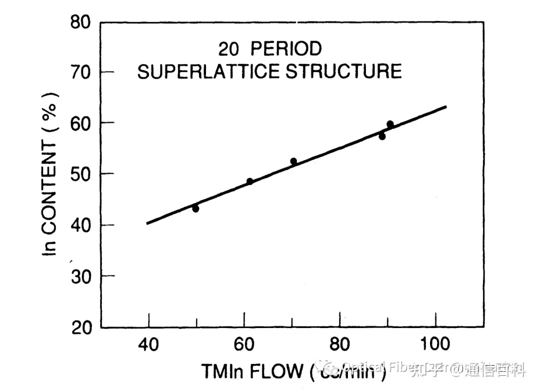
For a layer lattice-matched to InP, the In content is 53%. The data were obtained from a superlattice sample grown by atmospheric-pressure MOVPE on a (100)-oriented InP substrate, containing 20-50 periods of strained quantum wells separated by 20 nm thick InP barriers. Judging from the sharp and strong satellite peaks in the X-ray diffraction measurement, the strained layer maintained structural integrity. The linear relationship between the TMIn flux and the solid In composition in In1−xGaxAs indicates that TMIn fully decomposes at the growth temperature (625°C) and is proportionally incorporated into the epitaxial In1−xGaxAs layer.
Using MBE and MOVPE growth techniques, strained In1−xGaxAs layers have been grown on GaAs substrates. When grown by MBE, RHEED (reflection high-energy electron diffraction) oscillations can be used to monitor the growth front in situ. The three figures below show the RHEED oscillations in three cases:
- Growing GaAs on GaAs;
- Growing In0.3Ga0.7As on GaAs;
- Growing In0.5Ga0.5As on GaAs.
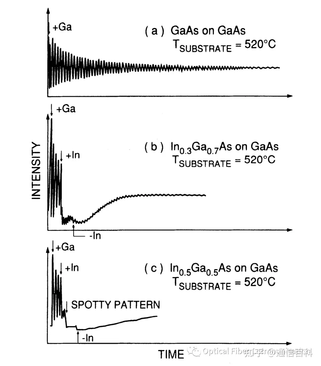
In the figure, “+” and “-” indicate the addition or removal of these substances. For example, +Ga means turning on the Ga beam at the indicated time. (a) corresponds to lattice-matched growth, where the RHEED oscillations show smooth layer-by-layer growth. However, in the strained case (when the In source is turned on), the growth mode rapidly transitions to a mode indicating island formation, that is, the RHEED oscillations disappear. Figure (c) indicates that as the strain increases (higher In mole fraction), the transition to the island growth mode becomes more abrupt.
Related Reading
- What is the Difference Between a Semiconductor Substrate and an Epitaxial Layer?
- How to Couple VCSEL Light into the PIC Wafer Plane?
- 2024 Semiconductor Industry Research Report – Automotive-Grade Chips
Enjoy this article?
Subscribe to get new optical communication insights delivered to your inbox. Free, unsubscribe anytime.