In the 1980s and early 1990s, significant progress was made in optical and electronic integration technologies that integrate semiconductor lasers and other related devices onto a single chip.
These chips enable a higher level of functionality than individual devices. For example, lasers and electronic driver circuits have been integrated to serve as simple monolithic optical-wave transmitters. Likewise, photodetectors have been integrated with amplifier circuits based on field-effect transistors (FET) or heterojunction bipolar transistors (HBT). Such integrated devices can serve as the front end of a receiver.
Optoelectronic integration is not only a technical achievement in photonics but also promises to reduce system cost.
We should know that the name photonic integrated circuit (PIC) is generally used when all integrated components are photonic devices, such as lasers, detectors, amplifiers, modulators, and couplers. The name optoelectronic integrated circuit (OEIC) is used for the combination of photonic and electronic devices.
Today, let us first look at what array technology in photonic integrated circuits (PIC) is like.
The simplest photonic integrated circuit is a one-dimensional array composed of lasers, light-emitting diodes, or photodetectors. These devices are fabricated exactly the same way as individual devices, except that the wafer is left in strip form rather than being scribed in the manner of individual device chips.
The schematic of a laser array is shown in Figure 1 below, which shows respectively a schematic and a photograph of an independently addressable edge-emitting laser array. Individual elements are isolated by etching V-shaped grooves between the emitters. The array consists of channeled-substrate buried-heterostructure (CMBH) lasers.


Laser or light-emitting-diode arrays can be used as light sources for dense parallel optical interconnection, a technology that can be applied to next-generation computing and switching systems.
A necessary condition for array technology is low power consumption and no crosstalk between elements in the array. The former requirement arises from the limited thermal-conduction capability of transmitter and receiver modules under typical operating conditions and environments.
If low-threshold lasers are used, the power-consumption problem is greatly reduced. We have already fabricated such lasers (with a threshold current of about 1 mA) for the AlGaAs and InGaAsP material systems. In both cases, the lasers have multi-quantum-well (MQW) active regions, short cavity lengths, and high-reflectivity facet coatings.
The fabrication of laser and detector arrays enables them to operate at data rates up to 1.4 Gb/s without crosstalk.
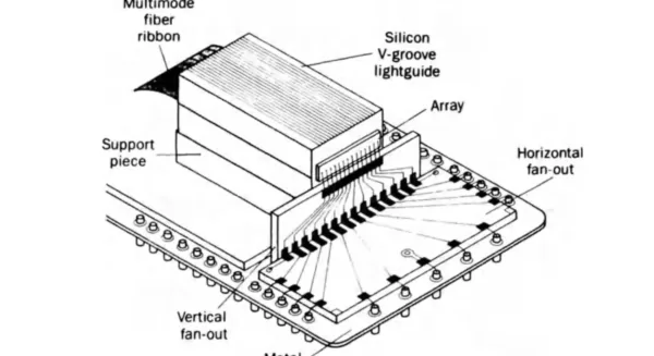
LEDs and photodiodes are packaged into 1×12 arrays, using a 12-fiber bundle and silicon V-grooves for alignment. The end of the fiber bundle is a connector consisting of silicon V-grooves with a center-to-center spacing of 250 μm. Schematics of the LED and laser array packaging are shown in Figure 2(a)(b).

Figure 2 (a)

Figure 2 (b)
The two figures above show packaging schematics of (a) LED and (b) edge-emitting laser arrays for parallel optical interconnection, respectively. The packaging uses a 60 μm-core 1×12 multimode fiber bundle, connected to V-grooves on a silicon block.
For two-dimensional emitter arrays, surface-emitting laser technology is a natural extension of surface-emitting LED array technology, offering higher speed and power levels. Independently addressable two-dimensional arrays of surface-emitting lasers have been reported.

Related Reading
- How to Couple VCSEL Light into the PIC Wafer Plane?
- Interposer, Silicon Bridge, and PIC/EIC Stacking Solutions
- Using Silicon Photonic Modules as a Guinea Pig?
Enjoy this article?
Subscribe to get new optical communication insights delivered to your inbox. Free, unsubscribe anytime.