If you are interested in semiconductors / chips / optical device modules / optical fiber communication, etc.
Welcome to follow us!
The development of AI, especially large models, has placed unprecedented demands on the data transmission capability of data centers.
This demand, which we call Scale Up, is different from the traditional Scale Out. The core of Scale Up lies in tightly connecting thousands upon thousands of GPUs to form a massive collaborative computing unit.
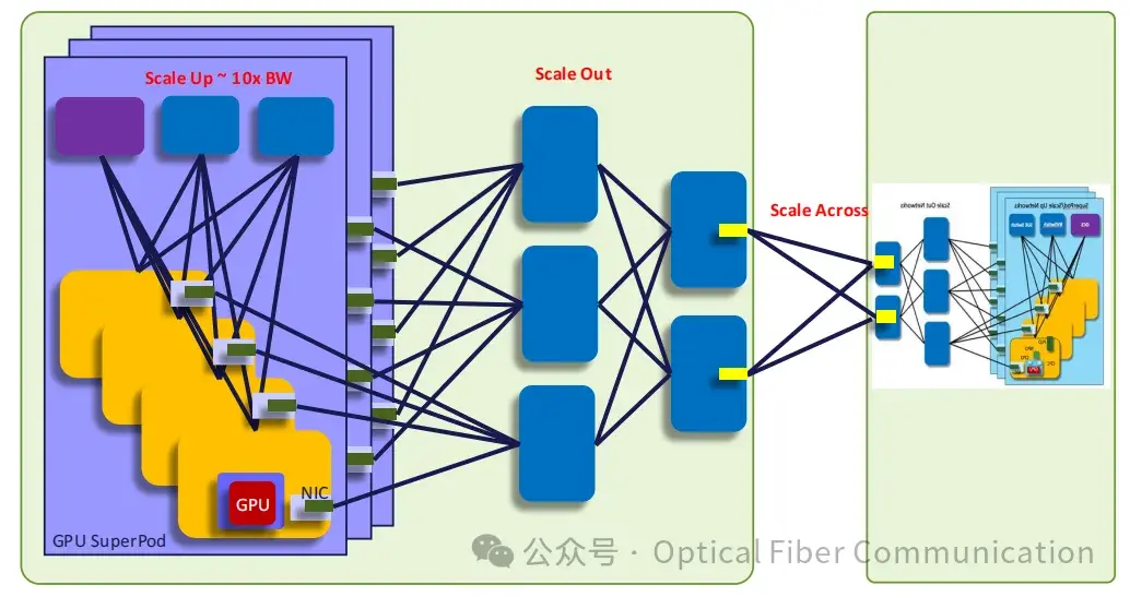
So, what are the specific requirements of Scale Up on the network?
First, it is bandwidth. This demand is very significant, requiring roughly a 10-fold increase. For example, for NVIDIA’s GB200 superchip, the internal interconnect bandwidth required by each GPU is as high as 7.2 Tbps, far exceeding the current 800 G level of our network cards.
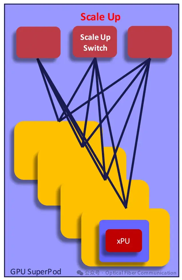
Second, it is connection distance and type. When computing expands from a single cabinet to multiple cabinets, copper cables become inadequate, and we must turn to optical connections.
Third, it is reliability. With so many GPUs running as a whole, any problem in any link will affect the entire system, so stability is crucial.
Fourth, it is latency. To ensure the performance of the GPU SuperPod, low latency is a must, which requires high-performance, low-BER FEC technology.
Finally, of course, it is power consumption and cost. We hope the power consumption of optical modules is far lower than that of the GPU itself, with the ultimate goal of maximizing the computing efficiency produced per watt of power and per dollar of cost.
Speaking of the key technologies to achieve these goals, silicon photonics technology has already withstood the test of large-scale field deployment, proving its extremely high reliability.
The cumulative deployment time of some companies’ silicon photonics chips has exceeded 40 billion device-hours, with a very low FIT rate.
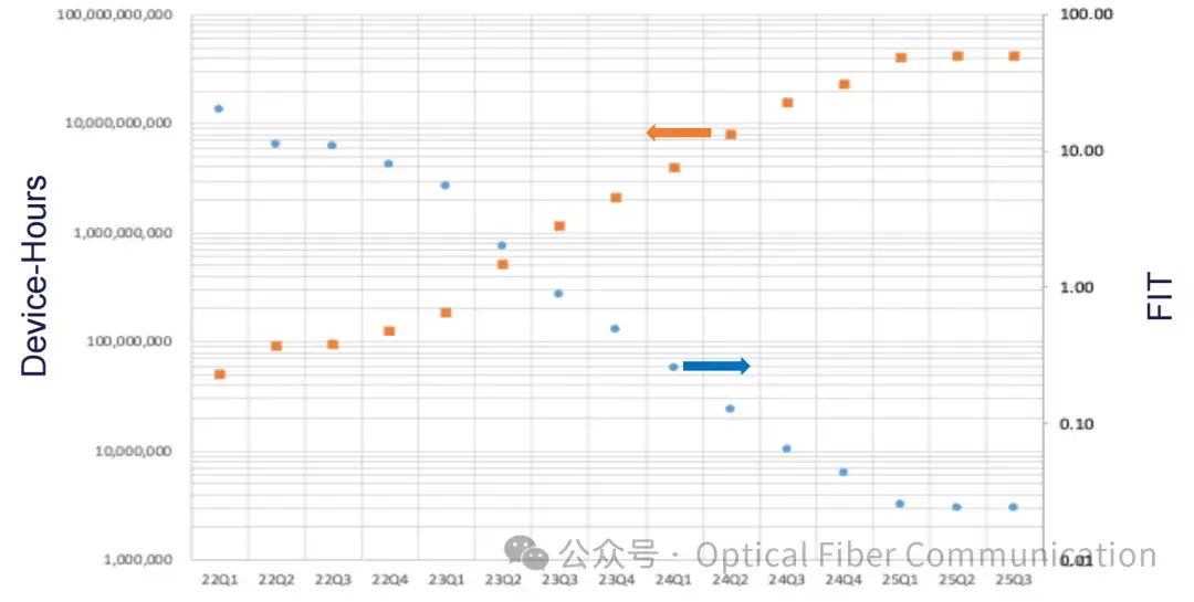
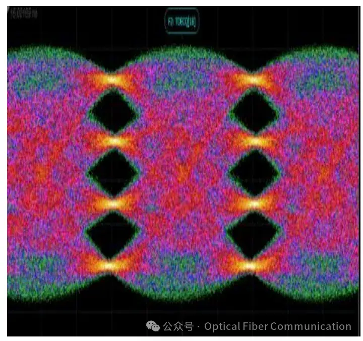
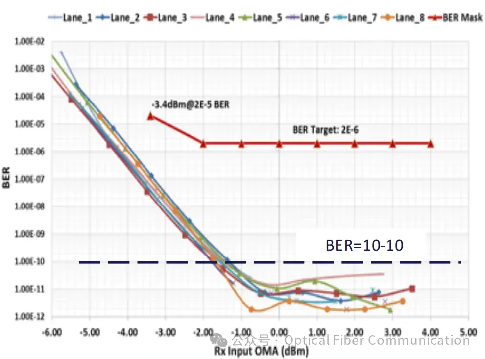
The 1.6T optical transceiver based on silicon photonics performs very stably under the 200 G PAM4 modulation format.
For more knowledge about 1.6T silicon photonics modules, you can refer to:
1.6T/3.2T Optical Modules: Half-DSP, Half-LPO Hybrid Architecture
ByteDance & Xihe: 1.6T LPO Views and Implementation Path
1.6T DR8 Optical Engine and Coupling Methods
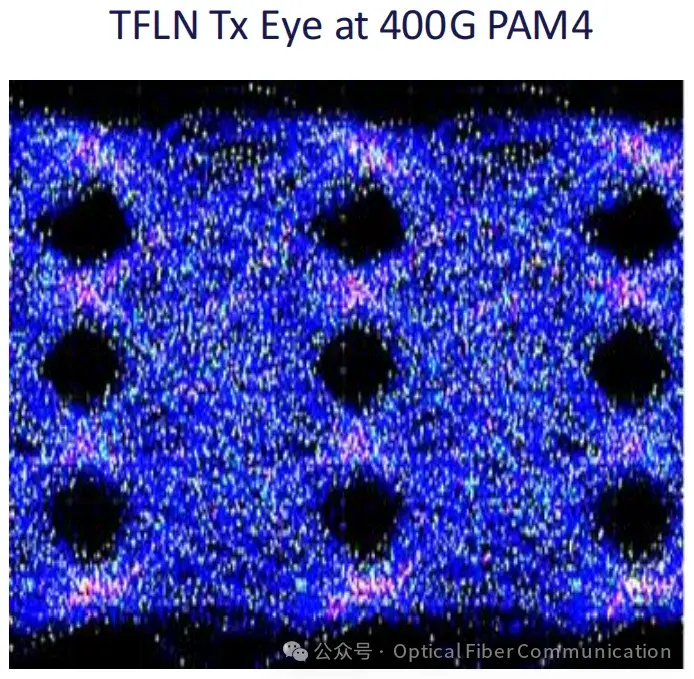
Moreover, the hybrid silicon photonics solution combined with the new material TFLN has broad prospects and is expected to further raise the single-channel rate to 400 G PAM4.
Let us look at the evolution of the optical module itself.
Pluggable optical modules, which we often call PLO, are still the mainstay at present.
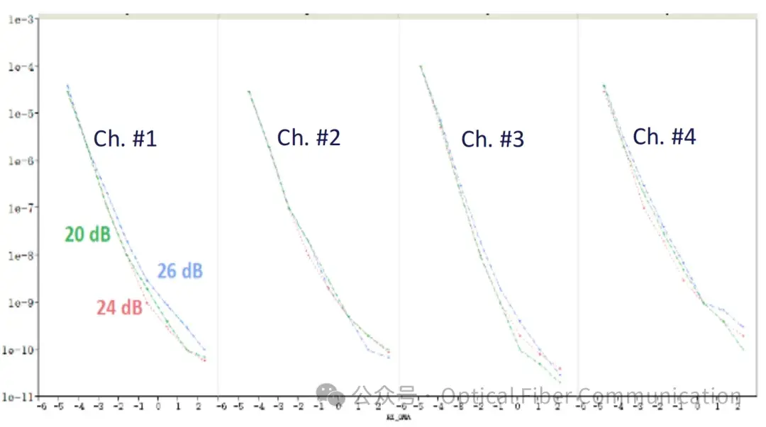
Early tests using commercial switches showed good results, with an extremely low BER floor.
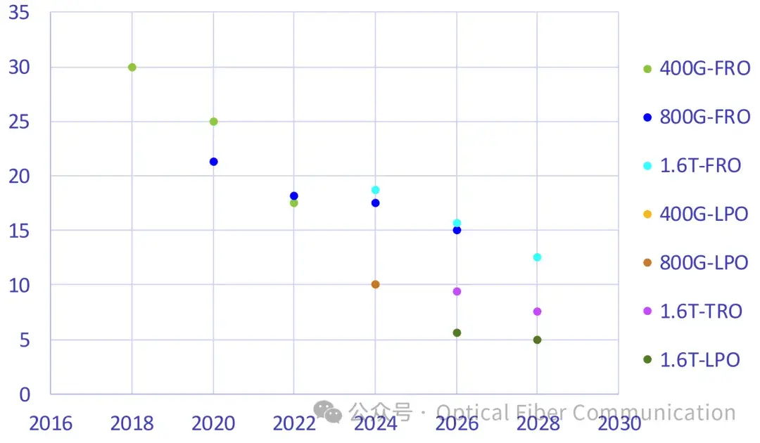
At the same time, its power consumption continues to decrease. As DSP chip process technology advances to 3nm or even 2nm, the power consumption of 1.6T modules can be reduced to below 16 W, with energy efficiency below 7.5 pJ/b. If the linear direct-drive technology LPO is adopted, it is even expected to reach 5 pJ/b, which is of great significance for reducing the total power consumption of data centers.
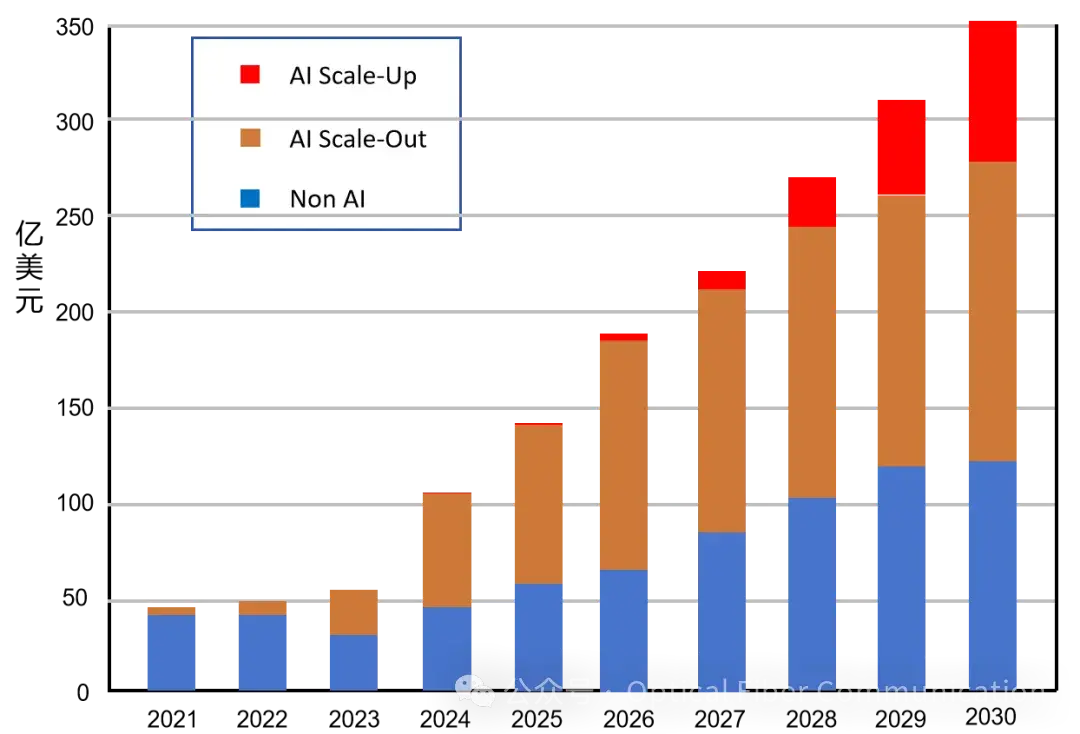
In addition to power consumption, cost is also of great concern. According to industry forecasts, the price of pluggable optical modules will continue to decline, and it is expected that by 2030, the per-Gbps cost of 1.6T modules will be below 0.1 US dollars.
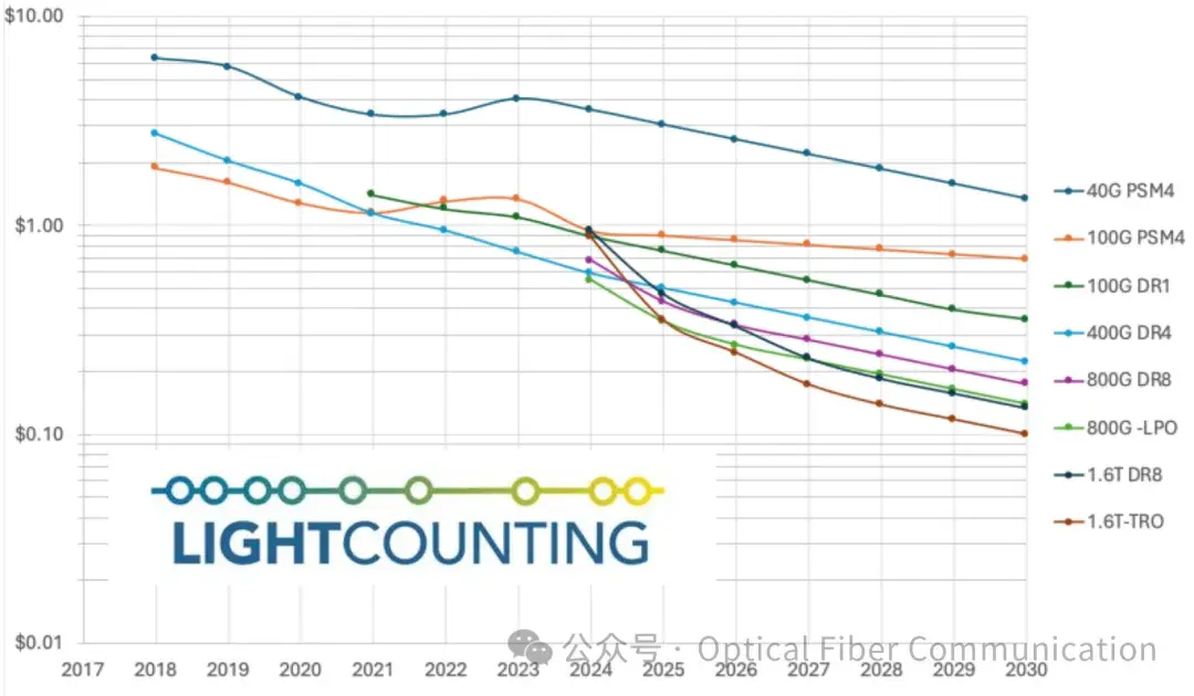
(From publicly available network information)
Through higher degrees of silicon photonics integration, such as making a 64-channel 200 G 12.8 T module, costs can be further optimized.
Taking the OIF high-density connector project as an example, its newly developed high-density 2D electrical connector has achieved breakthroughs in multiple aspects.
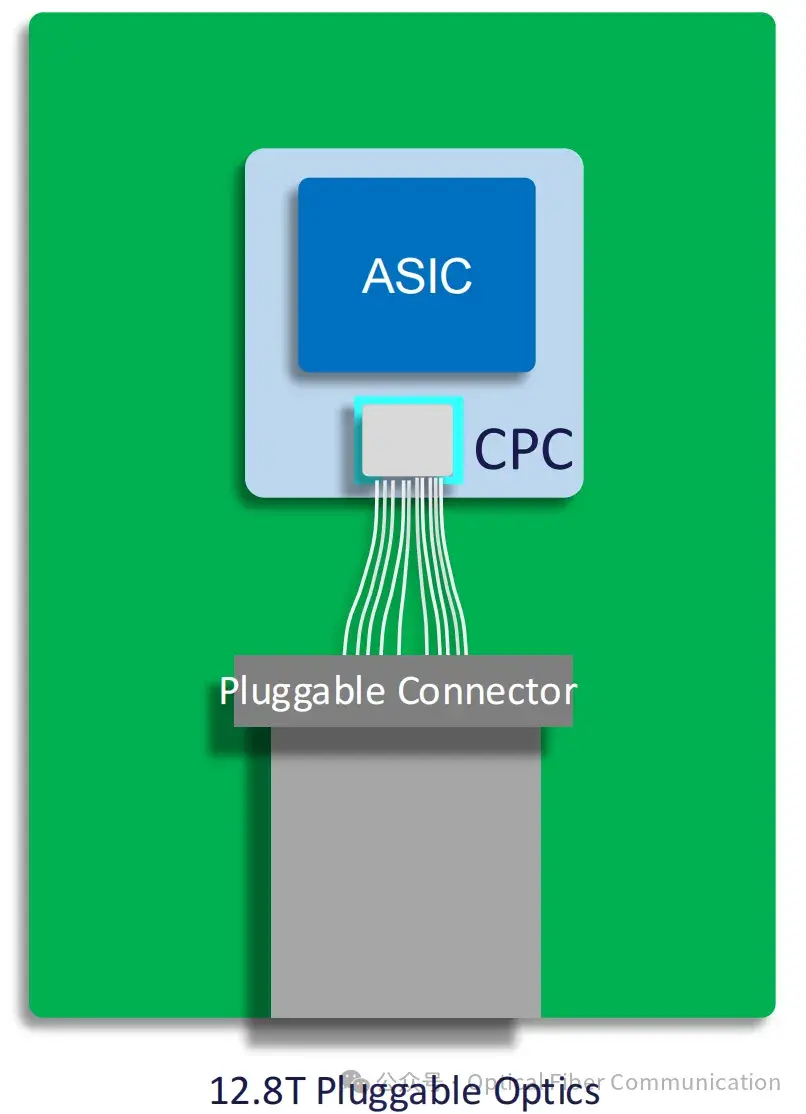
This high-density integration enables it to support 12.8 T or 25.6 T of bandwidth, with an I/O rate designed as high as 224 G PAM4, and can further evolve to 448 G PAM6 or PAM8 in the future. At the same time, its compact module size also fits well with GPUs and Scale-up switches.
Furthermore, due to the use of silicon photonics technology and a more simplified design, its reliability is higher and the BOM count is lower. Combined with a low-power solution, it can achieve a lower $/Gbps.
So, how will the future of optical interconnect technology evolve? At present, there are three main paths.
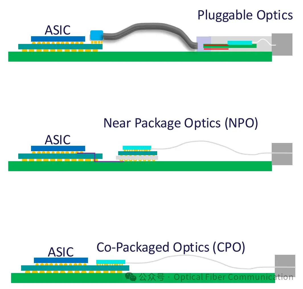
The first is to continue evolving PLO. Pluggable optics have an open ecosystem and are easy to maintain and replace. Through linear optics and CPC technology, low power consumption and high signal integrity are achieved, and the single-module transmission capacity can exceed 10 Tbps.
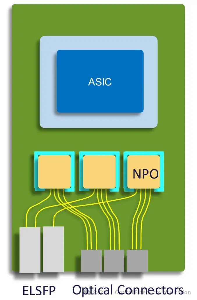
The second path is near-package optics, that is, NPO. It places the optical engine closer to the ASIC, reducing electrical channel loss, while supporting the concept of Open Socket, making maintenance more convenient than the following solution.

The third path is CPO, which places the OE and ASIC on the same substrate, with the lowest electrical channel loss and the greatest performance potential.
But it requires binding early in development, with limited technology choices, and very high repair cost and difficulty, so it is still in the early stage. The industry is also considering whether Open CPO is possible.
For CPO reliability verification, you can refer to:
Broadcom: 51.2T CPO Reliability Data and 102.4T CPO Switch
Let us focus on the NPO path. Its Open Socket design is particularly promising. It is compatible with a variety of deployed high-speed connectors, which already support a rate of 200 G per channel.
So the greatest advantage of NPO is decoupling the ASIC interface from the specific choice of optical or copper connections, giving system designers great flexibility, while also promoting an open, multi-vendor ecosystem, with much lower cost and difficulty of repair and replacement.
For in-depth reading on NPO-related topics: Broadcom & HiSilicon: VCSEL NPO/CPO and Silicon Photonics CPO
Finally, let us summarize:
- PLO will continue to evolve, making continuous progress in cost, power consumption, and reliability;
- NPO, especially in the form of Open Socket, is a very promising next evolution direction, balancing performance and ecosystem health;
- CPO, although with great potential, is still in the early stage of development and faces many challenges.
Thank you for reading!
Reference: OCP2025-Optics for Scale Up.pdf
We invite you to join our community to obtain a large number of Ebooks, technical documents, and trend research reports in the fields of semiconductor chips / optical devices / optical modules!

Welcome to join the “Semiconductor/Optical Device Industry Chain Exchange Group (already 300+ people).” Please add WeChat “WaytoICT” and note your relevant industry direction.
Related Reading
- Pluggable, OBO, NPO and CPO
- Murata: NPO/CPO Technology Based on Low-Temperature Co-Fired Ceramics and Its Evolution Route
- Two Types of CPX Socket Interfaces Supporting NPO and CPO
Enjoy this article?
Subscribe to get new optical communication insights delivered to your inbox. Free, unsubscribe anytime.