Recently, CoWoP, which has appeared in NVIDIA’s technology roadmap, has become a hot topic in the semiconductor industry. So how exactly does it compare with the previously much-discussed CoWoS and CoPoS technologies? As we know, traditional 2.5D/3D packaging technologies usually use a “silicon interposer,” and achieve high-density interconnection between chips through the “through-silicon vias” (TSV)…
Technology
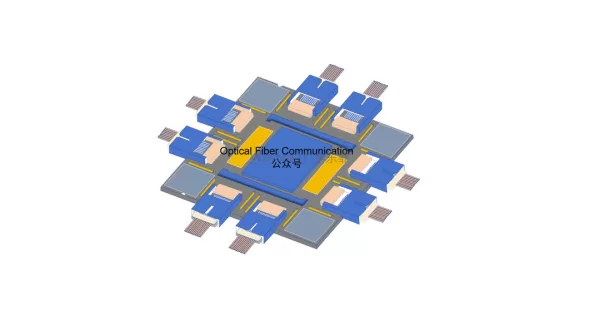
A CPO Optical Engine Package Structure with Pluggable Fiber
This is a WaytoICT paid-reading column. The full technical analysis and accompanying schematics require a ¥9.9 payment to unlock! In addition, during use, when the ambient temperature rises, the coefficient of thermal expansion mismatch between the silicon photonics chip and the PCB substrate also enlarges the optical alignment tolerance. This degrades the system’s maintainability and…
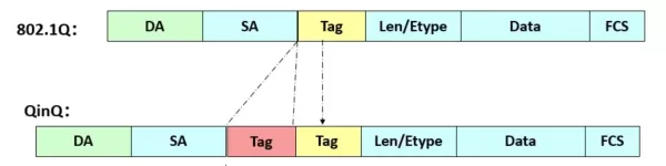
What Is QinQ? Why Do We Need QinQ?
In optical access networks, we often encounter QinQ applications. So what is QinQ? Why do we need QinQ? Let us summarize today. What is QinQ? QinQ is actually an extension technology of VLAN. As for what VLAN technology is, I believe many people are already very familiar with it, so we will skip it here….
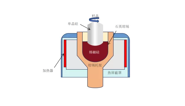
How Is a Silicon Wafer Actually Manufactured?
Silicon wafers are very familiar to those of us in the semiconductor industry. But in fact, they are thin slices cut from large single-crystal silicon grown from molten electronic-grade polysilicon. The process used to grow these single crystals is named after its inventor Jan Czochralski and is called the Czochralski process. The figure below shows…