Skip to content

WaytoICT

通往ICT之路 · 光通信与AI网络技术解读

中文English
登录注册
Menu
Technology Optical comms · silicon photonics · CPO → Market Insights Financials · trends · industry → In-Depth Analysis Optical chips, devices & modules → Video Understand a topic in minutes → Documents Latest docs · summit materials →
Menu

Technology

Silicon Photonics Series 2: What Is a Grating Coupler?

Posted on 2024-05-26 by

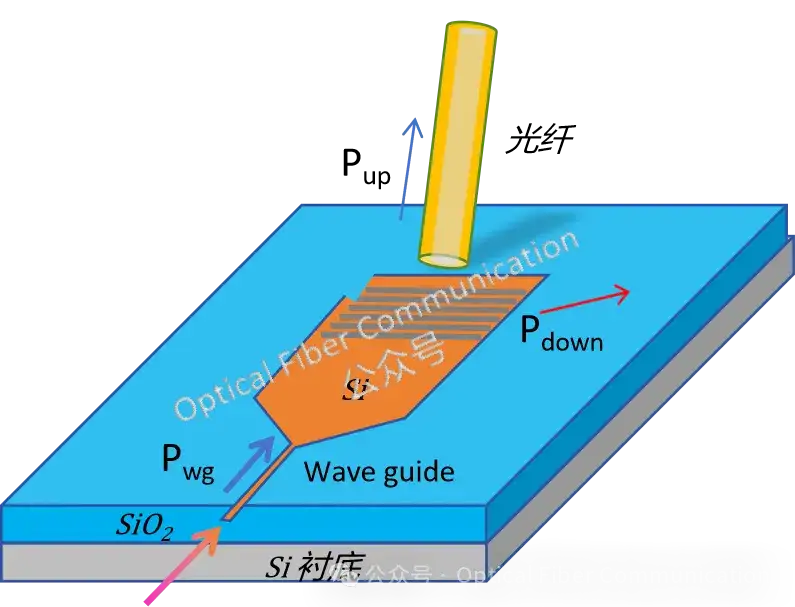
In the previous article, “Silicon Photonics Series 1: How to Smoothly Couple Light from Fiber into the Waveguide?“, we mentioned that a grating-coupling approach can be used. Below, let us look at what a grating coupler is. A grating coupler is an optical interface device that connects optical fiber or free space to a silicon-on-insulator…
Read more

Why Does Better Coherence Mean More Noise?

Posted on 2024-05-21 by

In the field of optical fiber communication, coherence is a very critical concept. It describes the consistency of light waves in time and space, that is, the frequencies, vibration directions, and phase differences of multiple light waves are all the same. When these light waves meet, interference occurs between them, such as mutual superposition or…

Read more

What Does the “0.13μm Process Capability” Refer To?

Posted on 2024-05-18 by

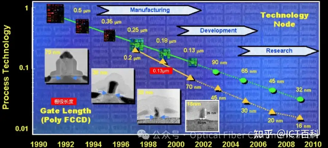
The 0.13μm process, in the semiconductor field, refers to the gate length of the transistor and represents a technology node. We know that the gate length directly affects the switching speed and current driving capability of the transistor, so generally we want the gate to be as short as possible. Being short has many benefits,…

Read more

What Is Nanoimprint Lithography? Will It Replace Photolithography?

Posted on 2024-05-15 by

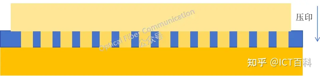
Nanoimprint lithography (NIL), also called NIP in some places, is a printing-and-replication technology used for transferring micro-nano electronic structures. It uses a patterned template to replicate micro-nano structures onto the material to be processed, stamping the pattern onto the material like a seal, similar to what we call embossing. Nanoimprint lithography was developed mainly because…

Read more
  • Previous
  • 1
  • …
  • 43
  • 44
  • 45
  • 46
  • 47
  • 48
  • 49
  • …
  • 72
  • Next

订阅更新

订阅后,新文章发布时第一时间收到邮件通知

李东霏
光互连技术研究者

香农信息技术研究院,专注光模块、CPO、硅光与 AI 光互连的技术解读。

行业报告

光芯片·光器件·光模块 2026 报告汇编(含 OFC 2026)

光芯片 · 光器件 · 光模块
2026 报告汇编(含 OFC 2026)

¥1,900

上/下两册,收录 OFC 2026 一线报告
添加微信 WaytoICT 订购

广告

📢 广告位招商:面向全球光通信客户 侧边栏广告位 Email:Dongfei.li@shannoninstitute.cn

最新文档

  • 互连拐点:11 页解析机架内到多机架 Scale-Up 的 XPO/CPX/OCI 蓝图(OCP 2026 全球峰会)
  • AI 时代的相干光技术:17 页解析 Scale-Across、液冷 XPO 与全谱转发器(OCP 2026 全球峰会)
  • XPO 高密度光互连的系统级评估:20 页解析 212G SerDes 平台与 FRO/LRO/LPO 实测(OCP 2026 全球峰会)
  • CPO 与 OCI 标准及未来技术:17 页 Broadcom 精简版演讲提纲(OCP 2026 全球峰会)
  • VCSEL 高密度互连:7 页解析 50G NRZ「慢而宽」阵列与光 PCIe 演示(OCP 2026 全球峰会)

最新评论

暂无评论,欢迎登录后发表第一条评论。

最近访客

👥 今日访客 -
加载中…
© 2026 WaytoICT | 蜀ICP备2020035321号-2 | 隐私政策 | 免责声明
Wechat Pay
Alipay
请使用 支付宝 或 微信 扫码支付