Since Bell invented the telephone in 1876, human communication has undergone earth-shaking changes. These changes have not only reshaped people’s communication patterns but also driven the continuous innovation of data transmission technology. For nearly a hundred years, whether wired telephones or wirelessly transmitted radio and television, analog signals were used to transmit signals for a…
Do You Know These Properties of Photoresist?
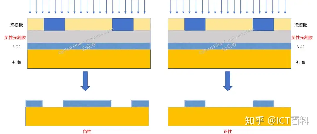
In our article the day before yesterday, “What Exactly Is a Photomask?”, we said that a photomask is like the “negative” of an old camera. In fact, the lithography field also has something similar to our “photographic paper,” namely the “photoresist.” Photoresist is coated onto the wafer and then exposed to light, “printing” the pattern…
What Is Wafer Thinning, and How Does It Differ from CMP and Grinding?
Someone in our community asked about “wafer thinning and CMP.” On the surface, CMP also has a thinning effect, but they are actually quite different. In addition, there is also a grinding/polishing process that may cause some misunderstanding. Let us talk about them together below. To more intuitively show the differences among these processes, let…
What Exactly Is a Photomask?
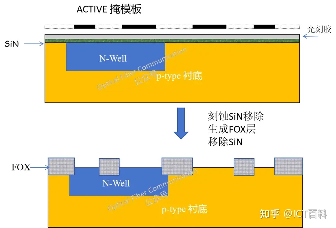
In the semiconductor field, a photomask is equivalent to the “negative” used by old cameras for taking photos. Lithography is performed on this “negative,” accurately transferring the pattern on it to the photoresist below. (Many post-90s and post-00s readers may never have come across this “negative” thing.) The materials used to make photomasks are mainly…