EUV photoresists are photosensitive materials used in semiconductor manufacturing processes, especially in advanced lithography technology. These materials must be able to withstand high-energy EUV photons and provide high-resolution patterning capability. Some of the challenges in developing EUV photoresist materials are that they need to be highly sensitive to short wavelengths; achieving high resolution is critical…

Center Wavelength/Frequency: What Is the Appropriate Spacing?
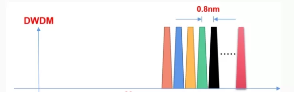
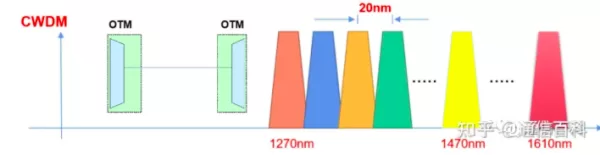
In the previous article, we discussed coarse wavelength-division multiplexing (CWDM) and dense wavelength-division multiplexing (DWDM). The channel spacing of CWDM is 20 nm, while DWDM has several channel spacings, with about 0.4 nm and about 0.8 nm being the most commonly used. Regarding wavelength, we know that temperature changes have a relatively large impact on…
What is Strained-Layer Epitaxy?
Although the growth of lattice-matched layers is very important for manufacturing reliable semiconductor lasers, we can also use materials with a small degree of lattice mismatch to manufacture high-quality semiconductor lasers. This lattice mismatch produces strain in the epitaxial layer, thereby changing the band structure of the semiconductor. The typical value of the tolerable strain…
Building Roads for Optical Fiber Communication (1)!
Preface: Regarding road building, as far back as the Shang Dynasty, people already knew to build roads with rammed earth so that oxen and horses could carry goods faster. The First Emperor even built a network of expressways leading to the whole country to mobilize troops faster, and I believe everyone has heard of the…